Patterning method

a technology of semiconductor and pattern, applied in the direction of decorative surface effects, electrical appliances, decorative arts, etc., can solve the problems of unfavorable anti-etching ability, unfavorable anti-etching effect, and inability to achieve the miniaturization of devices, so as to avoid reflection effect and enhance resolution without losing anti-etching ability

Active Publication Date: 2014-06-10
MACRONIX INT CO LTD
View PDF21 Cites 0 Cited by
  • Summary
  • Abstract
  • Description
  • Claims
  • Application Information

AI Technical Summary

Benefits of technology

[0007]The present invention provides a patterning method which can enhance the resolution without losing any anti-etching ability, and avoid the reflection effect in the lithography process, so as to fabricate a metal line with a line width less than 80 nm.
[0028]According to the patterning method of the present invention, a stop layer is disposed between the mask layer and the patterned photoresist layer to increase the resolution in a photolithography process as well as the anti-etching ability in an etching process. Therefore, the patterning method is beneficial for fabricating a line width less than 80 nm, and even for reducing critical dimensions of semiconductor devices.

Problems solved by technology

Hence, the miniaturization of devices can hardly be achieved by reducing the thickness of the photoresist layer directly.
Further, the incident light, which is through the photoresist layer and reflected from the substrate, interferes with a portion thereof, so as to cause a non-uniform exposure to the photoresist layer and result in a variation of critical dimensions.
For example, the incident light and the reflected light combine in the photoresist layer to create standing waves and cause distortions in the patterns of the photoresist layer; thus, the undesired change of a line width, such as necking or bridging and even photoresist collapse occurs.
Due to the above-mentioned problems, it is rather difficult when fabricating a metal line with a line width less than 80 nm.

Method used


Image

  • Patterning method
  • Patterning method
  • Patterning method

Examples


first embodiment

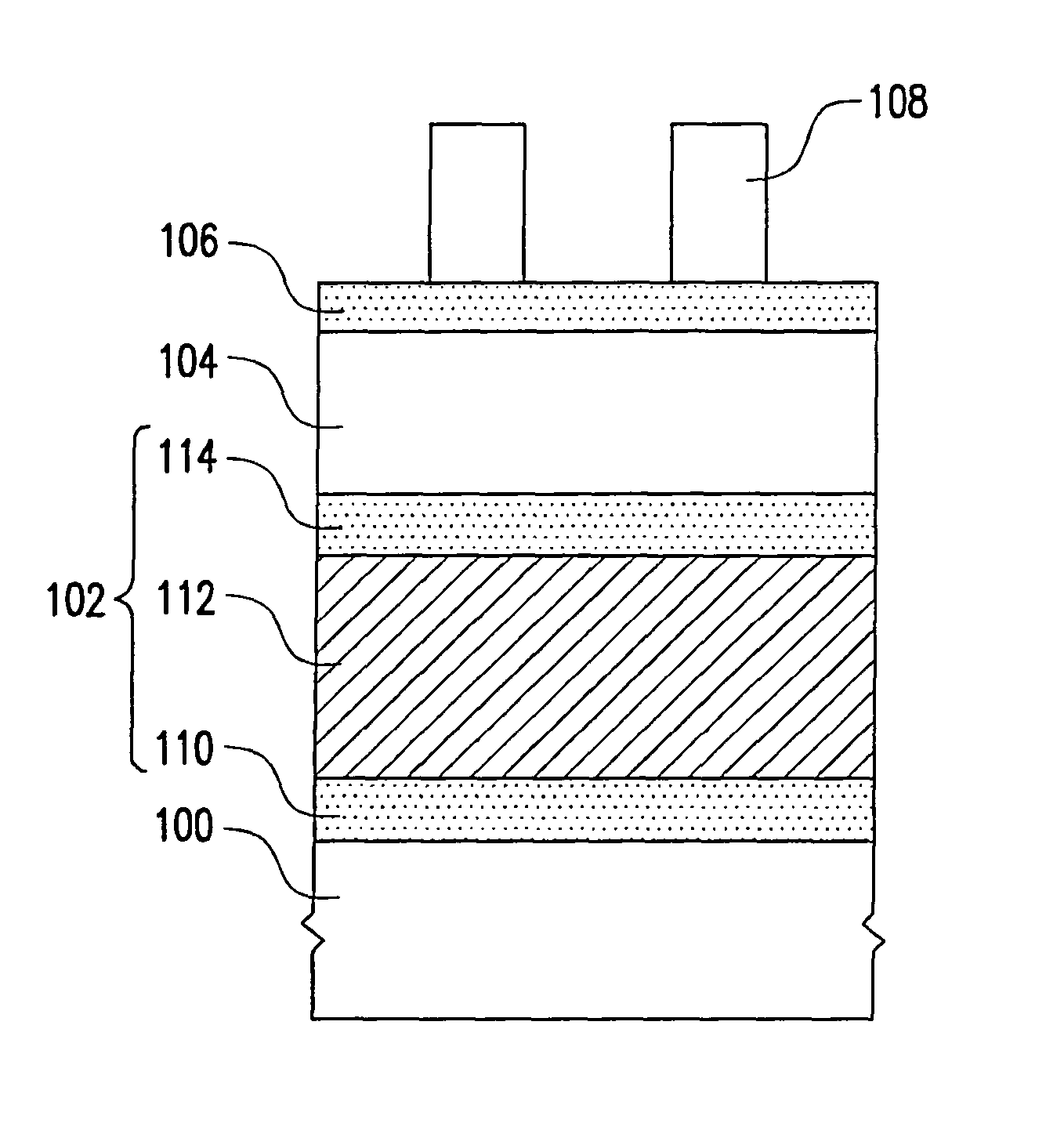
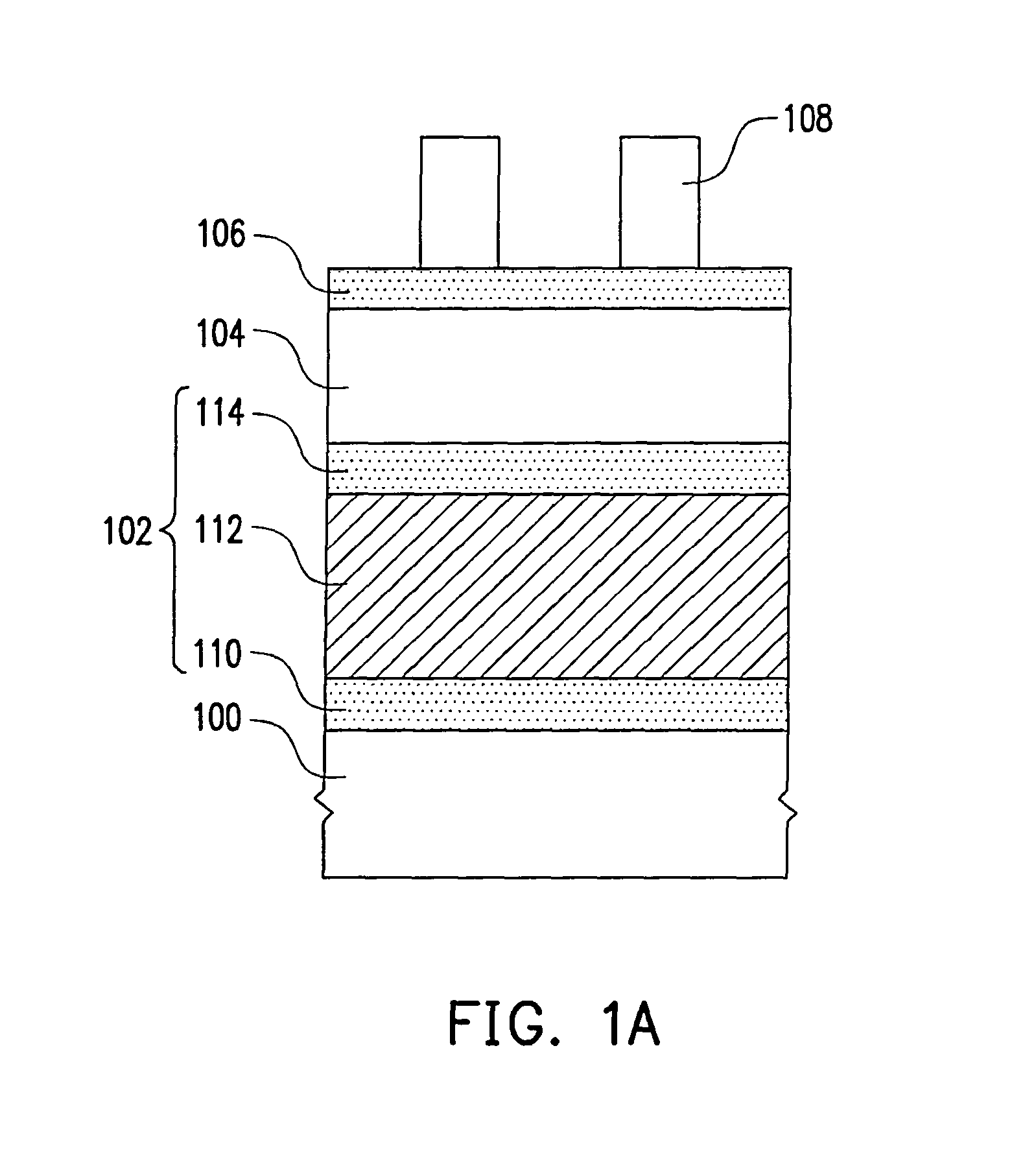
[0043]The present invention can be applied to the process of fabricating a line width less than 80 um, such as a metal line of 65 nm or 45 nm.

[0044]In this embodiment, a structure of FIG. 1A is formed first, wherein the objective material layer 102 may be a sandwich structure including a barrier layer 110, a metal layer 112 and an anti-reflection layer 114 which are sequentially formed on the substrate 100. The barrier layer 110, the anti-reflection layer 114 and the stop layer 106 may include the same material such as refractory metal, refractory metal nitride or combinations thereof. For example, the barrier layer 110 and the anti-reflection layer 114 include a material selected from the group consisting of Ti, TiN, Ti / TiN, Ta, TaN, Ta / TaN, W, WN and W / WN. The material of the metal layer 112 includes Cu, AlCu or AlSiCu, for example. The method of forming the barrier layer 110, the metal layer 112 and the anti-reflection layer 114 includes sputtering or CVD, for example. The materi...

second embodiment

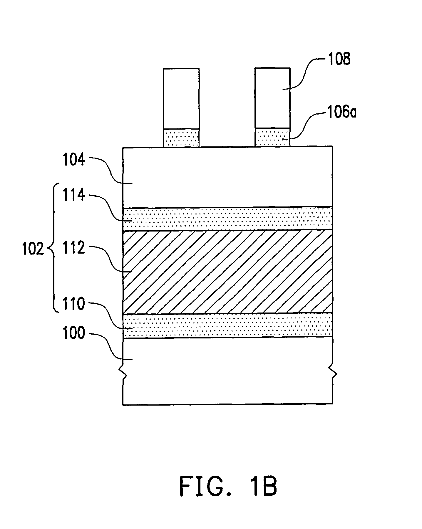
[0051]Like the first embodiment, the second embodiment is for fabricating a space less than 80 nm, especially for reducing a gap width by applying the patterning method of the present invention. FIGS. 1C′ to 1D′ schematically illustrate a cross-section view of a patterning method according to another embodiment of the present invention.

[0052]In this embodiment, a structure of FIG. 1B is formed first, wherein the materials and methods of forming the objective material layer 102 (including the barrier layer 110, the metal layer 112 and the anti-reflection layer 114), the patterned layer 106a and the patterned photoresist layer 108 are similar to the above-mentioned embodiments. It is noted that the material of the mask layer 104 of the second embodiment is different from that of the first embodiment. For example, the material of the mask layer 104 includes SiN or SiON.

[0053]Referring to FIG. 1C′, the mask layer 104 is etched, using the patterned layer 106a as a mask, to form a pattern...


PUM

PropertyMeasurementUnit
thicknessaaaaaaaaaa
thicknessaaaaaaaaaa
thicknessaaaaaaaaaa

Abstract

A patterning method is provided. First, a substrate having an objective material layer thereon is provided. Thereafter, a mask layer is formed on the objective material layer. Afterwards, a patterned layer is formed over the mask layer, wherein a material of the patterned layer includes a metal-containing substance. Then, the mask layer is patterned to form a patterned mask layer. Further, the objective material layer is patterned, using the patterned mask layer as a mask.

Description

BACKGROUND OF THE INVENTION[0001]1. Field of Invention[0002]The present invention relates to a semiconductor fabrication method, and more particularly to a patterning method.[0003]2. Description of Related Art[0004]The demand for a higher resolution in a photolithography process goes up as dimensions of semiconductor devices continue to shrink. Generally, the resolution increases as the thickness of a photoresist layer decreases. The photoresist layer, however, must have a thickness sufficient to resist etching (i.e. anti-etching ability). Hence, the miniaturization of devices can hardly be achieved by reducing the thickness of the photoresist layer directly.[0005]Further, the incident light, which is through the photoresist layer and reflected from the substrate, interferes with a portion thereof, so as to cause a non-uniform exposure to the photoresist layer and result in a variation of critical dimensions. For example, the incident light and the reflected light combine in the pho...

Claims


Application Information

Patent Timeline
Patent Type & Authority Patents(United States)
IPC IPC(8): H01L21/768H01L21/314H01L21/3105
CPCH01L21/31116H01L21/31138H01L21/76838H01L21/32139H01L21/32136
Inventor HSU, HAN-HUIHONG, SHIH-PINGWEI, AN-CHIWU, MING-TSUNG
Owner MACRONIX INT CO LTD
Why Eureka
Try Eureka