Wireless IC device

a technology of ic device and wire, applied in the direction of antenna details, instruments, antennas, etc., can solve the problems of module size and antenna radiation characteristic variation

Inactive Publication Date: 2014-06-24
MURATA MFG CO LTD
View PDF542 Cites 2 Cited by
  • Summary
  • Abstract
  • Description
  • Claims
  • Application Information

AI Technical Summary

Benefits of technology

[0007]In view of the above, preferred embodiments of the present invention provide a wireless IC device that is able to determine the size of a radiation plate and a radiation characteristic irrespective of an impedance of a wireless IC chip.

Problems solved by technology

Therefore, there has been a problem that the length of the loop antenna varies depending on the input impedance of an LSI used and, therefore, the size of the module itself and the antenna radiation characteristic vary.

Method used


Image

  • Wireless IC device
  • Wireless IC device
  • Wireless IC device

Examples


Embodiment Construction

[0027]Hereinafter, preferred embodiments of a wireless IC device according to the present invention will be described with reference to the accompanying drawings. Note that in the drawings, like reference numerals denote like components or portions, and the overlap description is omitted.

First Preferred Embodiment, See FIG. 1 to FIG. 4

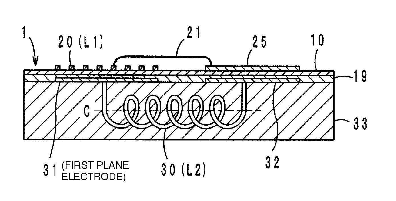
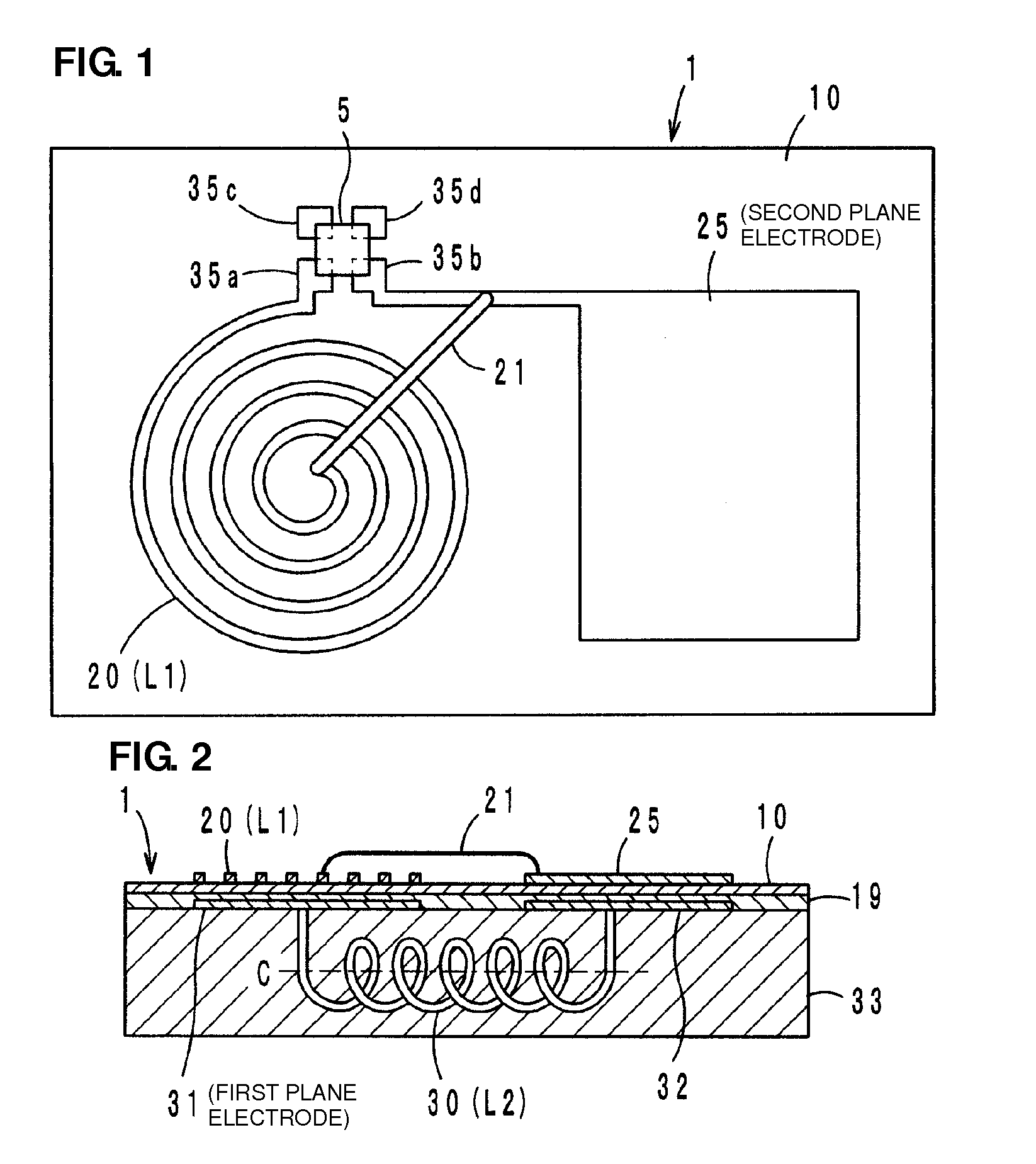
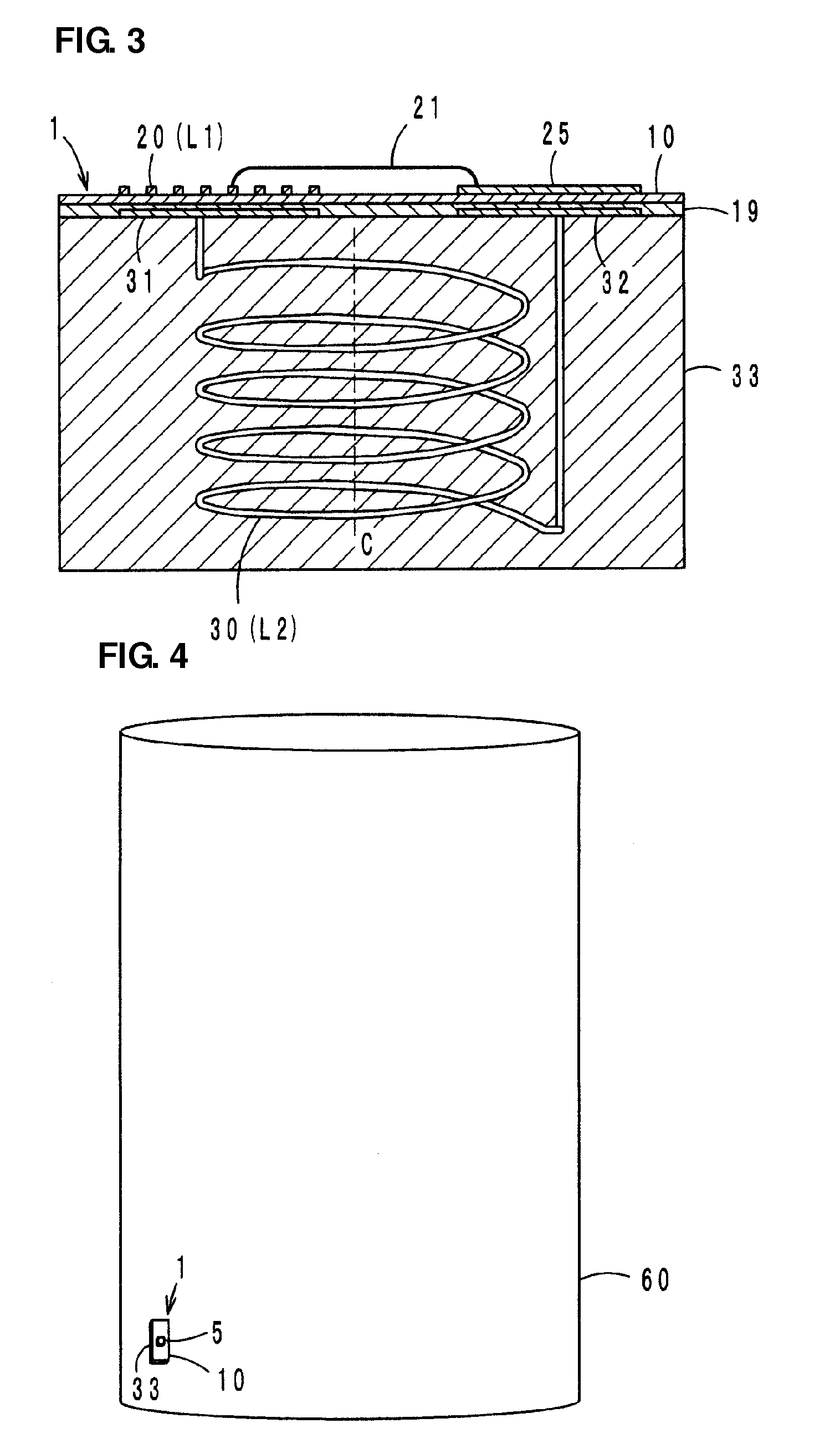
[0028]FIG. 1 and FIG. 2 show a wireless IC device according to a first preferred embodiment of the present invention. The wireless IC device includes a wireless IC chip 5, an inductance element 20 (L1), a plane electrode 25 (referred to as second plane electrode), and a coil-shaped radiation plate 30. The wireless IC chip 5 processes transmission and reception signals of a predetermined frequency. The inductance element 20 and the plane electrode 25 are disposed on a surface of the feeder circuit substrate 10, which is preferably made of a flexible dielectric (for example, PET film). The radiation plate 30 is preferably embedded in the radiation substr...


PUM


Abstract

A wireless IC device has a structure such that the size of a radiation plate and a radiation characteristic may be determined irrespective of an impedance of a wireless IC chip. The wireless IC device includes a wireless IC chip that is arranged to process transmission and reception signals, a spiral matching inductance element and a plane electrode that are located on a surface of a feeder circuit substrate, and a coil-shaped radiation plate located on a radiation substrate. Plane electrodes connected to both ends of the radiation plate are electromagnetically coupled respectively to the inductance element and the plane electrode. The wireless IC chip is operated by a signal received by the radiation plate, and a response signal from the wireless IC chip is radiated outside from the radiation plate.

Description

BACKGROUND OF THE INVENTION[0001]1. Field of the Invention[0002]The present invention relates to a wireless IC device and, more particularly, to a wireless IC device that includes a wireless IC chip used for an RFID (Radio Frequency Identification) system.[0003]2. Description of the Related Art[0004]In recent years, an RFID system has been developed as an article management system, which includes a reader / writer that generates an induction field and an IC chip (also referred to as IC tag or wireless IC chip) that stores predetermined information allocated to an article or a casing, and non-contact communication is established between the reader / writer and the IC chip to transmit the information therebetween. A known existing wireless IC device equipped with an IC chip includes a non-contact IC medium module described in Japanese Unexamined Patent Application Publication No. 2003-331246.[0005]The non-contact IC medium module is a combination of an LSI, a loop antenna and a capacitanc...

Claims


Application Information

Patent Timeline
Patent Type & Authority Patents(United States)
IPC IPC(8): G06K19/06
CPCG06K19/07749G06K19/07779G06K19/07783G06K19/07784H01Q1/2225H01Q1/40H01Q7/00
Inventor KATO, NOBORUDOKAI, YUYA
Owner MURATA MFG CO LTD
Why Eureka
Try Eureka