Supercharge Your Innovation With Domain-Expert AI Agents!

Photoelectric conversion device

a conversion device and photoelectric technology, applied in the direction of sustainable manufacturing/processing, climate sustainability, semiconductor devices, etc., can solve the problem of not being able to enhance the overall power production efficiency of the integrated modules and achieve the effect of improving the photoelectric conversion efficiency of the photoelectric conversion devi

Active Publication Date: 2014-06-24
SANYO ELECTRIC CO LTD
View PDF9 Cites 0 Cited by
  • Summary
  • Abstract
  • Description
  • Claims
  • Application Information

AI Technical Summary

Benefits of technology

This configuration improves photoelectric conversion efficiency by ensuring a more uniform distribution of electricity production across the substrate plane, enhancing overall power production efficiency without increasing the thickness of the amorphous silicon unit and reducing light deterioration.

Problems solved by technology

For this reason, there has been a problem in that it is impossible to enhance overall power production efficiency in the integrated modules of the photoelectric conversion device.

Method used


Image

  • Photoelectric conversion device
  • Photoelectric conversion device

Examples


Embodiment Construction

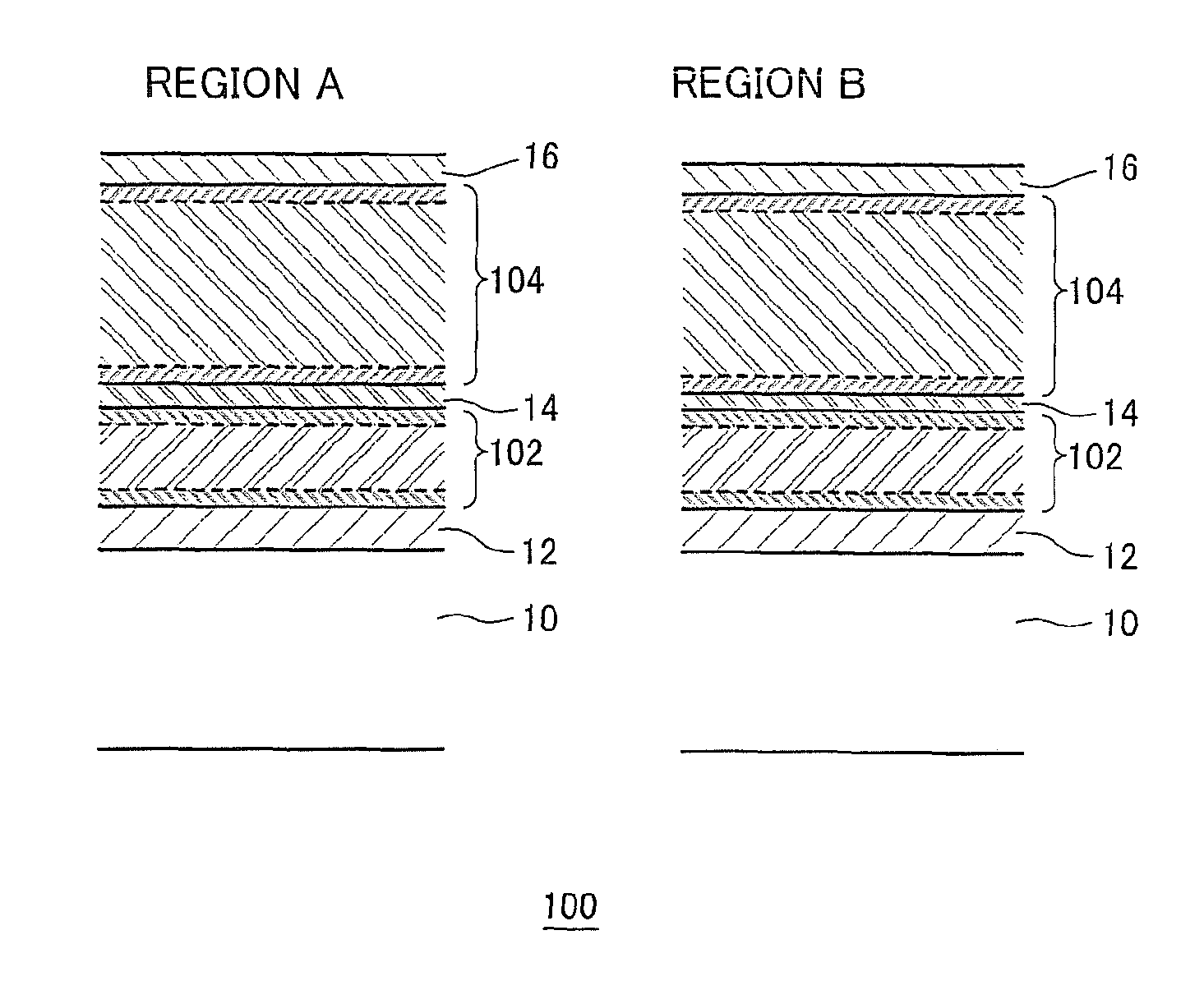
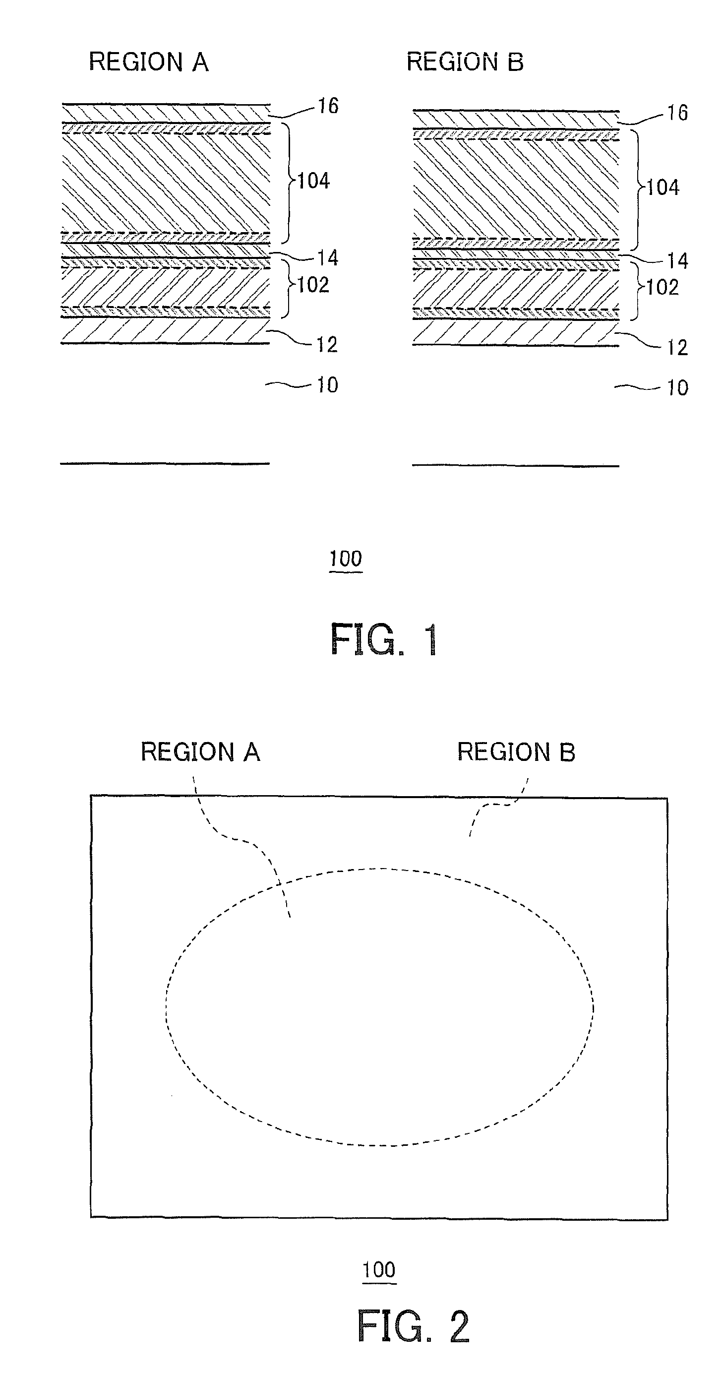
[0013]FIG. 1 is a cross sectional view showing a structure of a photoelectric conversion device 100 according to an embodiment of this invention. The photoelectric conversion device 100 in this embodiment has a laminated structure formed on a transparent insulating substrate 10, which is defined as a light incident side. The laminated structure is composed of, from the light incident side, a transparent conductive layer 12, an amorphous silicon (a-Si) (photoelectric conversion) unit 102 functioning as a top cell with a wider band gap, an intermediate layer 14, a microcrystalline silicon (μc-Si) (photoelectric conversion) unit 104 functioning as a bottom cell with a band gap narrower than that of the a-Si unit 102, and a back electrode layer 16, in that order. It should be noted that FIG. 1 shows both a region A, which is a high crystallization region of an i-type layer in the μc-Si unit 104 and will be described below, and a region B which is a low crystallization region of the i-ty...


PUM


Abstract

Disclosed is a photoelectric conversion device with improved photoelectric conversion efficiency. In the disclosed photoelectric conversion device, an amorphous silicon photoelectric conversion unit with an amorphous i-type layer and a microcrystalline silicon photoelectric conversion unit with a microcrystalline i-type layer are laminated, and an intermediate layer, which is disposed between the amorphous silicon photoelectric conversion unit and the microcrystalline silicon photoelectric conversion unit, has a lower refractive index than the layers in contact with the front or back surfaces thereof, wherein the higher the crystalline fraction of the microcrystalline i-type layer in the panel surface, the thicker the film of the intermediate layer.

Description

CROSS-REFERENCE TO RELATED APPLICATIONS[0001]The present application is a continuation application of International Application No. PCT / JP2011 / 060047, filed Apr. 25, 2011, the entire contents of which are incorporated herein by reference and priority to which is hereby claimed. The PCT / JP2011 / 060047 application claimed the benefit of the date of the earlier filed Japanese Patent Application No. 2010-103482 filed Apr. 28, 2010, the entire contents of which are incorporated herein by reference, and priority to which is hereby claimed.BACKGROUND[0002]1. Technical Field[0003]The present invention relates to a photoelectric conversion device.[0004]2. Related Art[0005]There have been known solar cells using polycrystalline, microcrystalline, or amorphous silicon. In particular, photoelectric conversion devices of laminated structure in which thin films of microcrystalline or amorphous silicon are laminated have been receiving attention, in view of resource consumption, cost reduction, and...

Claims


Application Information

Patent Timeline
Patent Type & Authority Patents(United States)
IPC IPC(8): H01L31/00
CPCH01L31/076H01L31/1824H01L31/202Y02E10/545Y02E10/548Y02P70/50
Inventor YATA, SHIGEO
Owner SANYO ELECTRIC CO LTD
Features
  • R&D
  • Intellectual Property
  • Life Sciences
  • Materials
  • Tech Scout
  • Unparalleled Data Quality
  • Higher Quality Content
  • 60% Fewer Hallucinations
Learn More