Methods for interconnecting bonding pads between components

a technology of interconnection and bonding pads, which is applied in the direction of printed circuit manufacturing, semiconductor/solid-state device details, manufacturing tools, etc., can solve the problems of many fabrication facilities not being equipped to handle all needed processes and materials, digital fabrication cost directly related to the chip, and the cost per chip area of analog fabrication can be significantly lower than the same chip area for digital fabrication, so as to achieve more cost-effective products

Inactive Publication Date: 2014-06-24
TERECIRCUITS CORP
View PDF22 Cites 60 Cited by
  • Summary
  • Abstract
  • Description
  • Claims
  • Application Information

AI Technical Summary

Benefits of technology

[0005]The present invention relates to processes and structures of integrated circuits (IC), particularly to radio frequency identification (RFID) tags, and more specifically to passive (non-powered) RFID tags. In an embodiment, the present invention discloses methods and apparatuses for the separations of IC fabrication and assembling of separated IC components to form complete IC structures. In the fabrication of IC devices, various fabrication processes and materials are not compatible, and many fabrication facilities are not equipped to handle all needed processes and materials. The present fabrication separation of an IC structure into multiple discrete components can take advantages of dedicated IC fabrication facilities and achieve more cost effective products.

Problems solved by technology

In the fabrication of IC devices, various fabrication processes and materials are not compatible, and many fabrication facilities are not equipped to handle all needed processes and materials.
In many cases, digital fabrication cost is thus directly related to the chip size.
However, the cost per chip area for analog fabrication can be significantly lower than a same chip area for digital fabrication.

Method used


Image

  • Methods for interconnecting bonding pads between components
  • Methods for interconnecting bonding pads between components
  • Methods for interconnecting bonding pads between components

Examples


Embodiment Construction

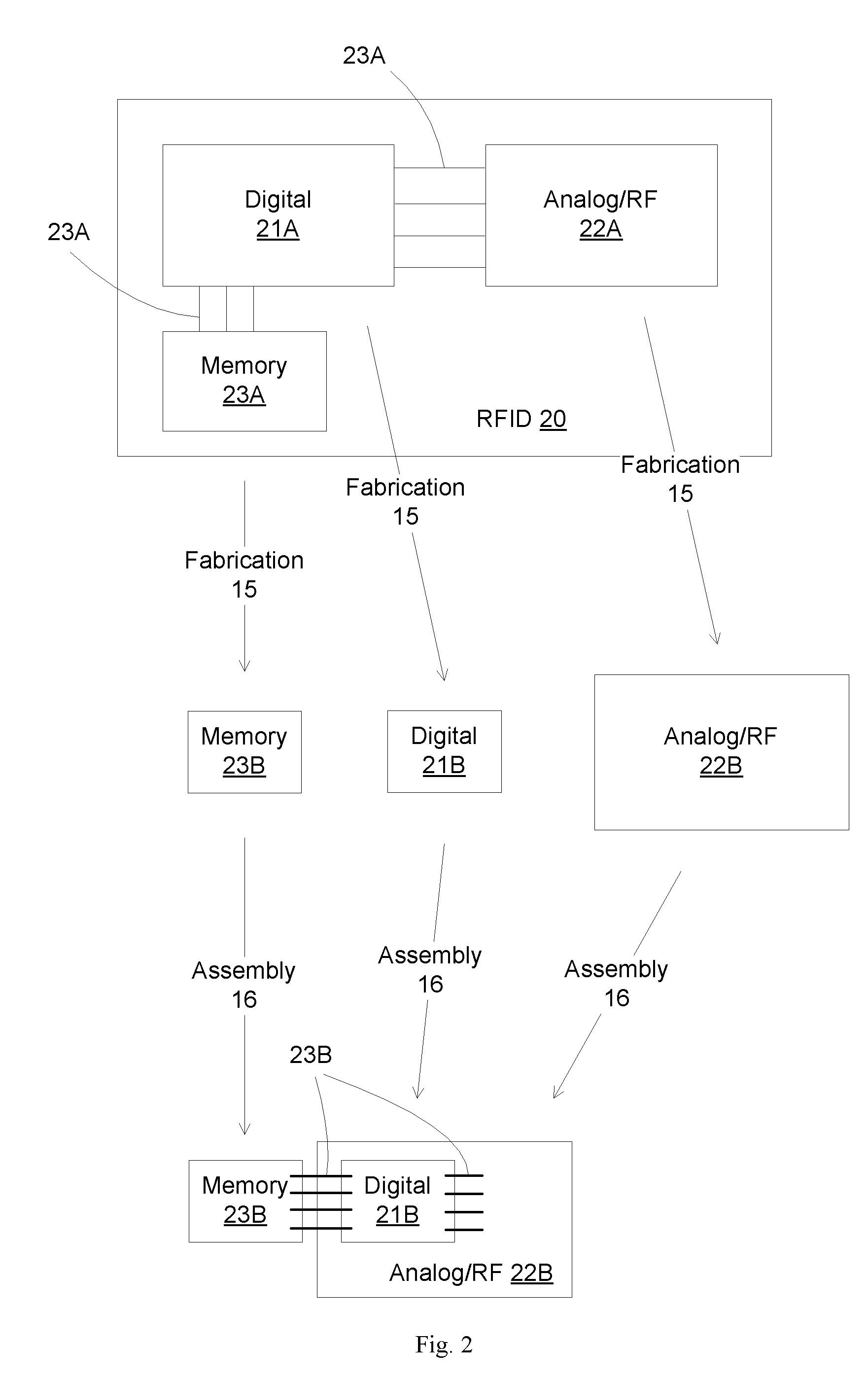
[0054]The present invention discloses processes and structures of integrated circuits (IC) fabrication. The following description relates to radio frequency identification (RFID) tags, but the present invention is not limited to RFID.

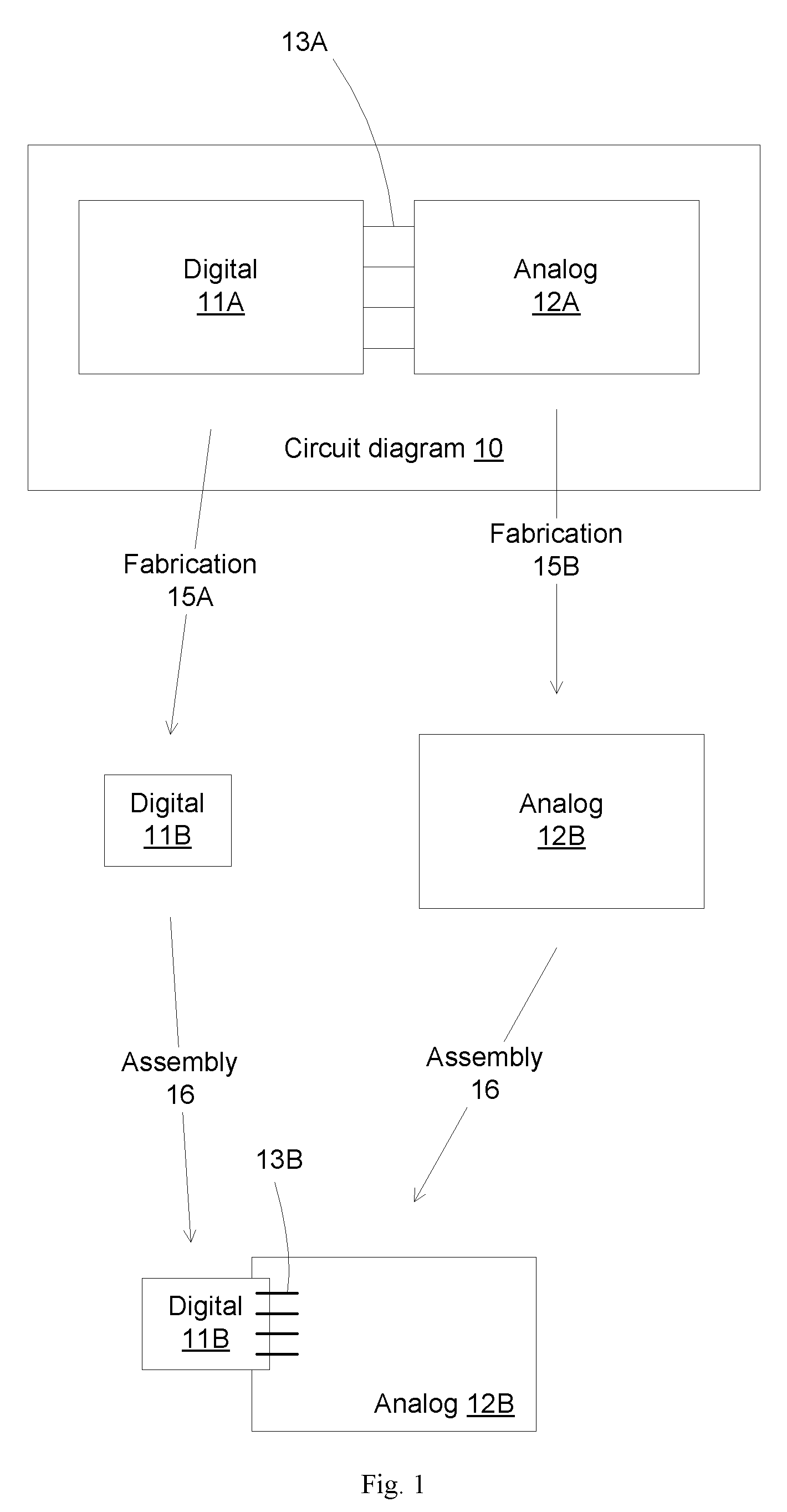
[0055]In an embodiment, the present invention separates the analog portion from the digital portion of an IC circuit for fabrication. FIG. 1 illustrates an exemplary process and structure for separating a circuit diagram 10 into separate digital component 11B and analog component 12B before assembling together to form a complete IC chip. A circuit design 10 can have a digital portion 11A and an analog portion 12A, connected through interconnection 13A. A separation process separates the portions of the circuit design, according to predetermined criteria, for example, to achieve a low cost of final product. The digital 11A and analog 12A are fabricated separately in different fabrication facilities 15A and 15B, to produce a digital component 11B and an a...


PUM

PropertyMeasurementUnit
areaaaaaaaaaaa
thicknessaaaaaaaaaa
capacitanceaaaaaaaaaa

Abstract

The present invention discloses methods and apparatuses for the separations of IC fabrication and assembling of separated IC components to form complete IC structures. In an embodiment, the present fabrication separation of an IC structure into multiple discrete components can take advantages of dedicated IC fabrication facilities and achieve more cost effective products. In another embodiment, the present chip assembling provides high density interconnect wires between bond pads, enabling cost-effective assembling of small chip components. In an aspect, the present process bonds multiple interconnect wires to bond pads with electrical linkages between the bond pads and then subsequently separates the adjacent bond pads.

Description

[0001]The present invention relates to co-pending applications “Processes and structures for IC fabrication” of the same inventor.BACKGROUND[0002]RFID tags are a class of integrated circuits which intercept modulated RF signals from a transmitter (which is normally called a “reader”), demodulate the signal and apply the encoded information to a digital portion of the circuit, and radiate a modulated signal to the reader. The signal typically contains only a small amount of information such as the identification number of the device, although more information may be stored in the tag's memory and may be used either to determine whether the tag responds, or to influence the string of bits which are applied to the modulator. The modulator alters the Q of the antenna and thus its normally re-radiated signal, so no active power is applied to the transmission.[0003]Such tags are intended to be applied to a very large number of objects, for example to shipping boxes or even to the individu...

Claims


Application Information

Patent Timeline
Patent Type & Authority Patents(United States)
IPC IPC(8): B23K26/38
CPCH01L29/0657H01L2224/05599H01L2924/01006H01L2924/30105H01L2924/01075H01L2924/00014H01L2224/48699H01L2224/49175H01L24/78H01L2224/48091H01L25/18H01L2924/01047H01L2224/78301H01L2224/45139H01L2924/01013H01L2924/10253H01L2924/14H01L2225/06524H01L2225/06513H01L2924/01078H01L2224/45147H01L2924/12032H01L2224/85214H01L24/49H01L23/5389H01L2924/01031H01L2224/45124H01L2924/01028H01L2224/45111H01L2225/06506H01L2224/48799H01L24/85H01L2924/19042H01L2224/85001H01L2224/48137H01L2924/10329H01L2924/01082H01L2225/06579H01L2924/01027H01L2924/01015H01L2224/45015H01L2224/48472H01L2924/014H01L2924/10157H01L24/48H01L2924/01014H01L2924/01023H01L2924/0105H01L2924/19043H01L2924/19041H01L2924/01029H01L24/46Y10T29/49147H01L2224/45014H01L2924/12043H01L2224/85205H01L2224/05554H01L2924/20752H01L2224/78H01L2924/00H01L2224/45099H01L2224/85399H01L2924/206
Inventor SHEATS, JAYNA
Owner TERECIRCUITS CORP
Why Eureka
Try Eureka