Reference voltage generation circuit and method

a reference voltage and circuit technology, applied in the direction of ac network voltage adjustment, transmission system, instruments, etc., can solve the problems of large power consumption and circuit area, large structure, and severe affecting the accuracy of output reference voltage and temperature coefficient, etc., to achieve low power consumption, simple structure, and small area

Active Publication Date: 2014-07-01
NOVATEK MICROELECTRONICS CORP
View PDF3 Cites 7 Cited by
  • Summary
  • Abstract
  • Description
  • Claims
  • Application Information

AI Technical Summary

Benefits of technology

[0007]The disclosure provides a reference voltage generation circuit and method. Since currents with temperature coefficients, rather than voltages, are used for subsequent processing, there is no need to implement buffers, and many advantages such as small area, low power consumption, simple structure, and accurate temperature coefficient may thus be achieved in the disclosure.

Problems solved by technology

However, due to having the buffers, the conventional structure is too huge, and the power consumption and the circuit area are larger than other conventional circuits performing no temperature compensation.
Besides, the buffers used in the addition / subtraction of voltages will incur extra offset, further severely affecting the accuracy in the output reference voltage and the temperature coefficient.

Method used


Image

  • Reference voltage generation circuit and method
  • Reference voltage generation circuit and method
  • Reference voltage generation circuit and method

Examples


first embodiment

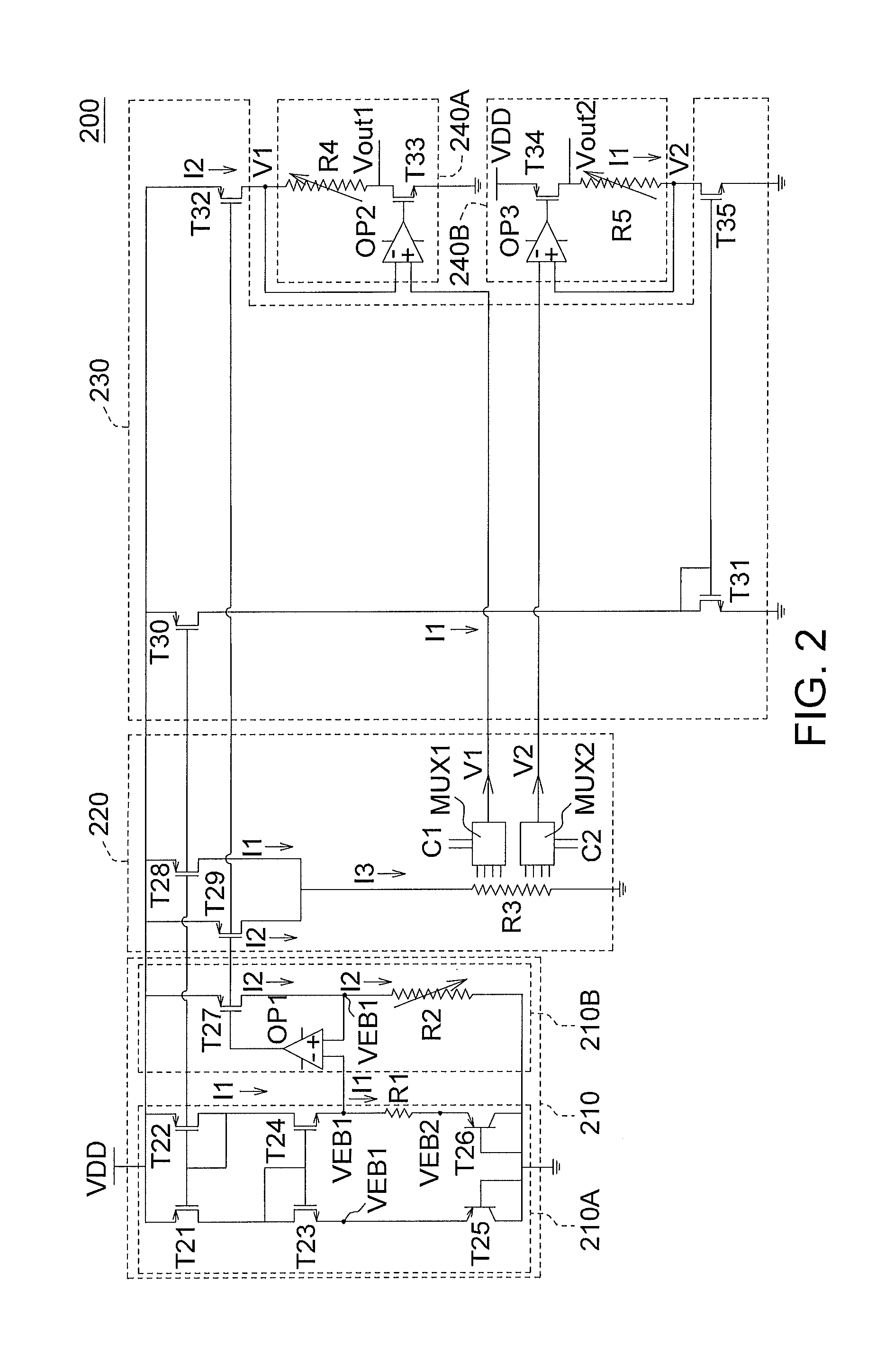
[0021]Referring to FIG. 2, a schematic diagram of a reference voltage generation circuit according to a first embodiment of the disclosure is shown. As indicated in FIG. 2, the reference voltage generation circuit 200 includes a bandgap reference circuit 210, a base voltage generation circuit 220, a bias current source circuit 230 and one or more regulating output circuits (exemplified by two regulating output circuits 240A and 240B). The following elaboration is also applicable to fewer or more regulating output circuits.

[0022]The bandgap reference circuit 210 may be used for generating initial currents with different temperature coefficients. Under exemplary conditions, the initial currents include a first current I1 with a positive temperature coefficient and a second current I2 with a negative temperature coefficient.

[0023]The base voltage generation circuit 220 is coupled to the bandgap reference circuit 210, for duplicating the initial currents generated by the bandgap referen...

second embodiment

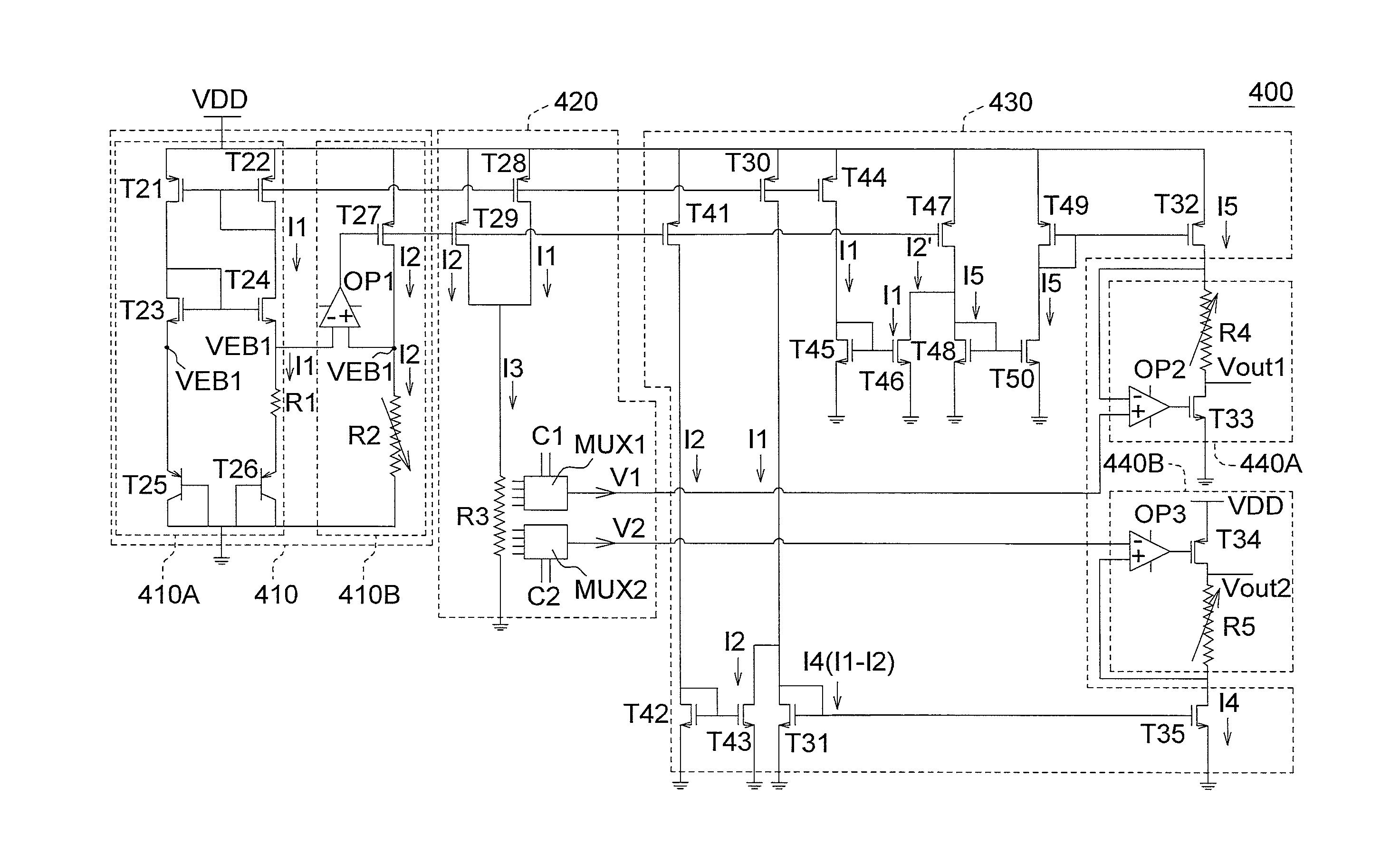
[0039]Referring to FIG. 4, a schematic diagram of a reference voltage generation circuit according to a second embodiment of the disclosure is shown. Similar to the reference voltage generation circuit 200 of FIG. 2, the reference voltage generation circuit 400 of FIG. 4 includes a bandgap reference circuit 410, a base voltage generation circuit 420, a bias current source circuit 430 and one or more regulating output circuits (exemplified by two regulating output circuits 440A and 440B).

[0040]In the exemplary example of FIG. 4, the bandgap reference circuit 410 further includes a PTAT current generation circuit 410A and a voltage-to-current conversion circuit 410B. The reference voltage generation circuit 400 of FIG. 4 is different from the reference voltage generation circuit 200 of FIG. 2 in that the bias current source circuit 430 not only duplicates the first and the second current I1 and I2 into bias currents but also has a current combining function to realize mathematical ope...

third embodiment

[0050]Referring to FIGS. 5A and 5B, which are schematic diagrams of a reference voltage generation circuit 500 according to a third embodiment of the disclosure are shown. Like the reference voltage generation circuit 400 of FIG. 4, the reference voltage generation circuit 500 of FIGS. 5A and 5B includes a bandgap reference circuit 510, a base voltage generation circuit 520, a bias current source circuit 530 and one or more regulating output circuits (exemplified by two regulating output circuits 540A and 540B). In the examples of FIGS. 5A and 5B, the bandgap reference circuit 510 further includes a PTAT current generation circuit 510A and a voltage-to-current conversion circuit 510B. The reference voltage generation circuit 500 of FIGS. 5A and 5B is different from the reference voltage generation circuit 400 of FIG. 4 in that the bias current source circuit 530 has a current path switching function so that the bias current may be flexibly switched between different temperature coef...


PUM


Abstract

A reference voltage generation circuit includes: a bandgap reference circuit, generating a plurality of initial currents with different temperature coefficients; a base voltage generation circuit, combining the initial current into a combined current, and converting the combined current into one or more base voltages; a bias current source circuit, generating one or more bias currents based on at least one of the initial currents; and one or more regulating output circuit, each converting a respective one of the one or more bias currents into an increment voltage and adding the increment voltage to the base voltage to generate a respective output voltage. Each output voltage may have its respective temperature coefficient.

Description

[0001]This application claims the benefit of Taiwan application Serial No. 99140101, filed Nov. 19, 2010, the subject matter of which is incorporated herein by reference.TECHNICAL FIELD[0002]The disclosure relates in general to a reference voltage generation circuit and method, and more particularly to a reference voltage generation circuit and method using a bandgap reference circuit.BACKGROUND[0003]Due to the characteristics of semiconductor, the output reference voltage of the reference voltage generation circuit has a temperature coefficient (abbreviated as TC) to compensate the temperature effect. For example, when an output reference voltage is 1.6V+10 mV / ° C., the absolute voltage of the output reference voltage is 1.6V at specified temperature (ex: 25° C.), and the temperature coefficient is 10 mV / ° C.[0004]FIG. 1A shows output reference voltages having different absolute voltage values, wherein curves A1, B1 and C1 respectively indicate that the output reference voltage is ...

Claims


Application Information

Patent Timeline
Patent Type & Authority Patents(United States)
IPC IPC(8): G05F3/26G05F1/577
CPCG05F3/30G05F3/242Y10T307/406G05F1/561
Inventor HU, MIN-HUNGWU, CHEN-TSUNGDING, ZHEN-GUOSU, PIN-HAN
Owner NOVATEK MICROELECTRONICS CORP
Why Eureka
Try Eureka