

Method for fabricating semiconductor device
a semiconductor and device technology, applied in the field of semiconductor device fabrication, can solve the problems of increasing the on-resistance of the power semiconductor, difficult to perform high aspect-ratio anisotropic etching, and difficult to form the epitaxial or drift region of the desired thickness, and achieves the effect of easy formation of a super junction structur
- Summary
- Abstract
- Description
- Claims
- Application Information
AI Technical Summary
Benefits of technology
Problems solved by technology
Method used
Image

Examples
Embodiment Construction
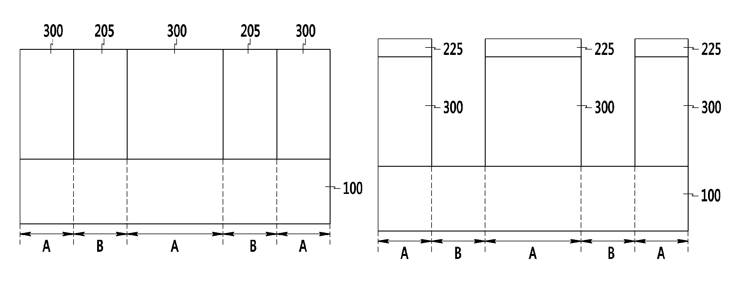
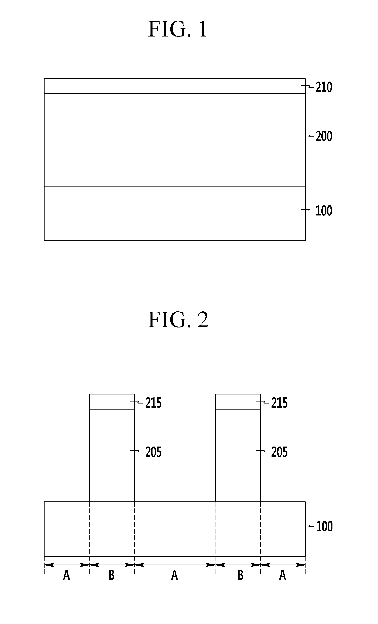
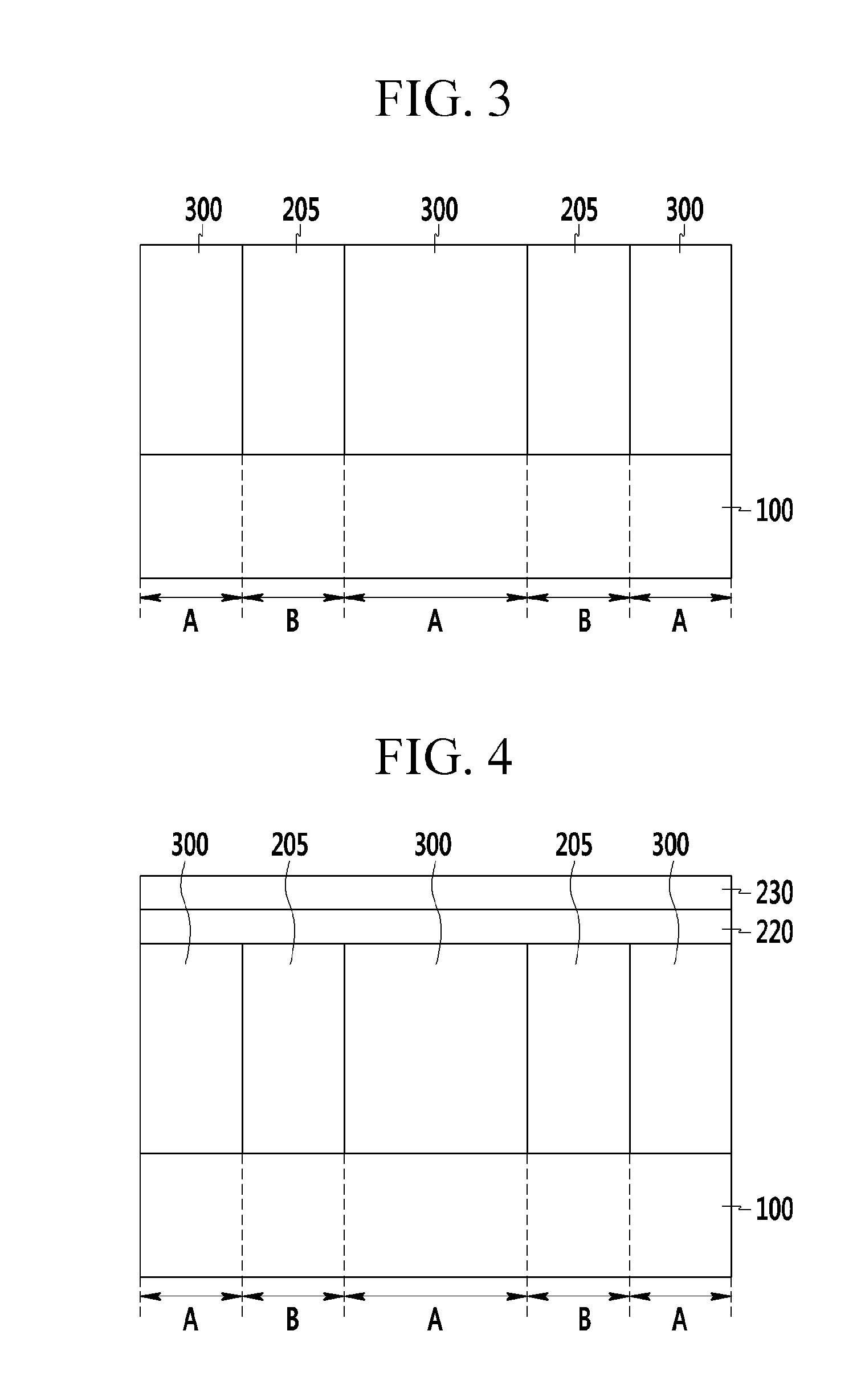
[0030]Exemplary embodiments of the present invention will be described in detail with reference to the attached drawings. The present invention may be modified in many different forms and should not be construed as being limited to the exemplary embodiments set forth herein. Rather, the exemplary embodiments of the present invention are provided so that this disclosure will be thorough and complete, and will fully convey the concept of the present invention to those skilled in the art.
[0031]In the drawings, the thickness of layers and regions may be exaggerated for clarity. In addition, when a layer is described to be formed on another layer or on a substrate, this means that the layer may be formed on the other layer or on the substrate, or a third layer may be interposed between the layer and the other layer or the substrate. Like numbers refer to like elements throughout the specification.
[0032]It is understood that the term “vehicle” or “vehicular” or other similar term as used ...
PUM
 Abstract
Description
Claims
Application Information