

High selectivity, low damage electron-beam delineation etch
a technology of electron beam and delineation etching, which is applied in the direction of basic electric elements, semiconductor/solid-state device manufacturing, electric devices, etc., can solve the problem that the reaction of rivals barely favors deposition on one or more of the other materials
- Summary
- Abstract
- Description
- Claims
- Application Information
AI Technical Summary
Benefits of technology
Problems solved by technology
Method used
Image

Examples
Embodiment Construction
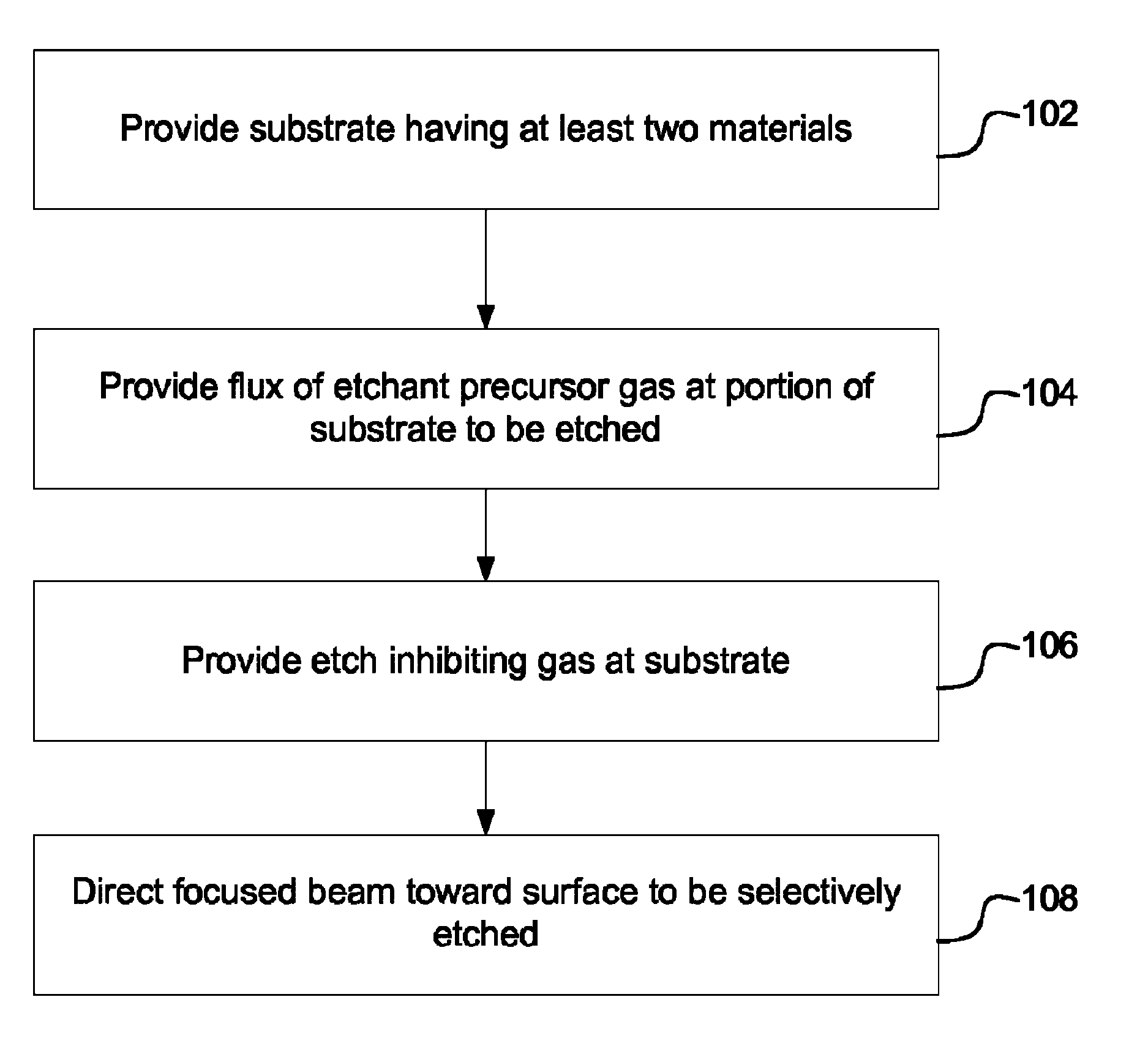
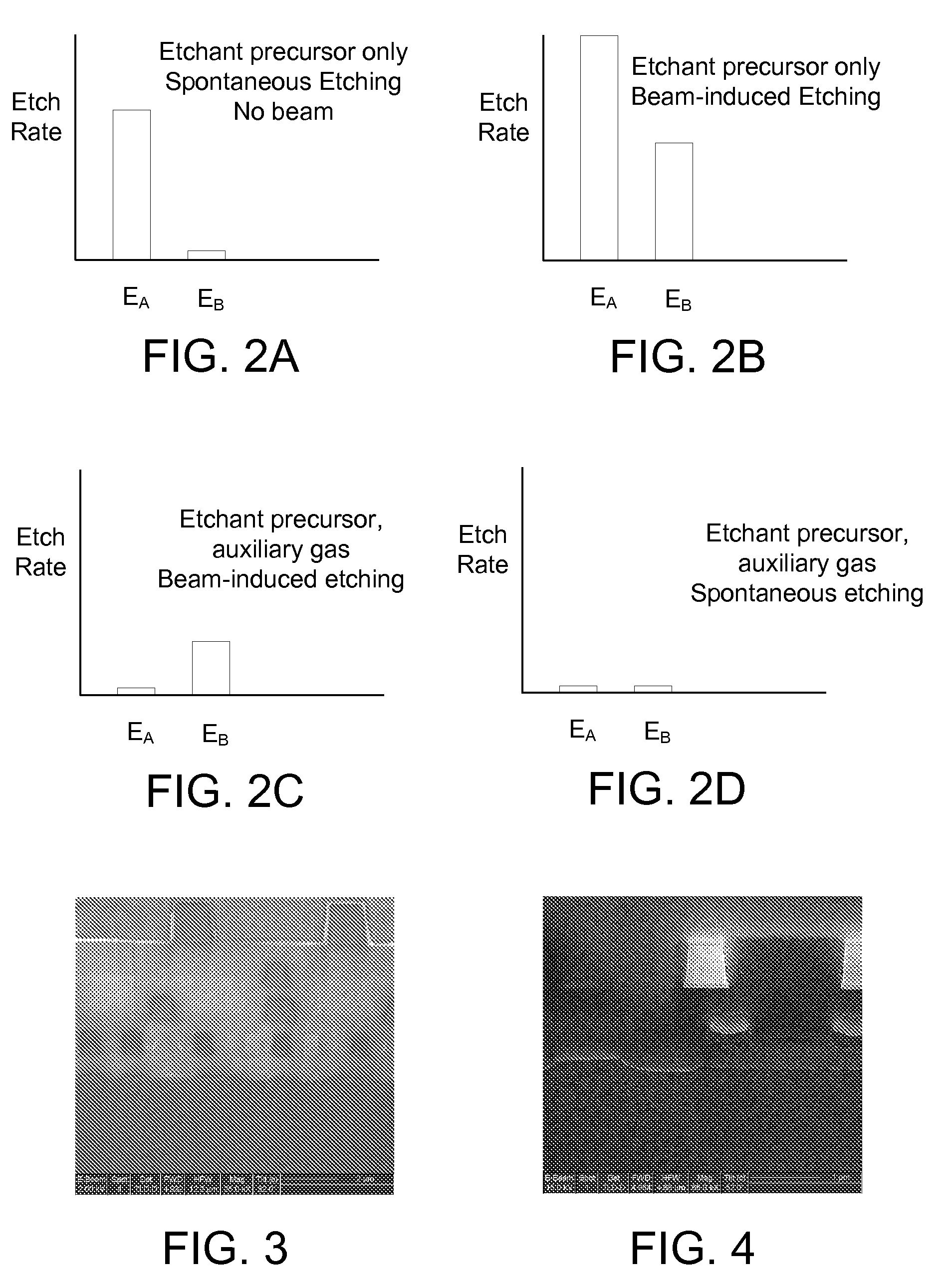
[0019]Embodiments of the invention provides a method and apparatus for selectively processing materials on a substrate using a focused beam, such as an electron beam, ion beam, neutral particle beam, or laser beam. Using a finely focused beam allows a user to precisely control the region to be processed. For example, modern electron beams can be focused to a spot size of a few nanometers and can be scanned over a region on the order of nanometers up to millimeters. During electron beam processing, a substrate typically has multiple materials exposed to the precursor gases or to the beam. In one preferred embodiment, competing reactions, both spontaneous and beam-induced, favor etching of a first material over etching of one or more other exposed materials. Thus, those embodiments preferentially etch the first material, while preserving or minimizing damage to the other exposed materials.
[0020]In some embodiments, two precursor gases are introduced into the region of the work piece. ...
PUM
 Abstract
Description
Claims
Application Information