Apparatus for a low-cost semiconductor test interface system

a test interface and low-cost technology, applied in the direction of electrical testing, instruments, measurement devices, etc., can solve the problems of not being able to expand the testing of the device under test, commercial test interface systems are not capable of testing both digital and analog devices, and without being substantially modified, so as to reduce the size of the test head

Inactive Publication Date: 2014-07-22
ALTERA CORP
View PDF9 Cites 1 Cited by
  • Summary
  • Abstract
  • Description
  • Claims
  • Application Information

AI Technical Summary

Benefits of technology

[0008]Broadly speaking, the present invention fills these needs by providing a module board that includes a flexible board section to allow bending of the module board to reduce the size of the test head and to enable use of mechanically efficient device interface board (DIB) interface connectors.

Problems solved by technology

Currently available commercial test-interface systems are incapable of being quickly adapted for testing of different types of devices and consequently do not allow for expanded testing of the device under test.
Moreover, commercial test-interface systems are not capable, without being substantially modified, of testing both digital and analog devices.
Furthermore, the mechanical design of commercial test-interface systems limits a use of high frequency clock for testing.
The Pogo pin connectors are expensive and have a short life span due to frequent pin bending and breakages.
The need for replacing these connectors considerably reduces overall efficiency of the testing system.
Furthermore, because test signals have to travel comparatively long distance, the clock frequency of the test signals is limited due to the length of the signal path.

Method used


Image

  • Apparatus for a low-cost semiconductor test interface system
  • Apparatus for a low-cost semiconductor test interface system
  • Apparatus for a low-cost semiconductor test interface system

Examples


Embodiment Construction

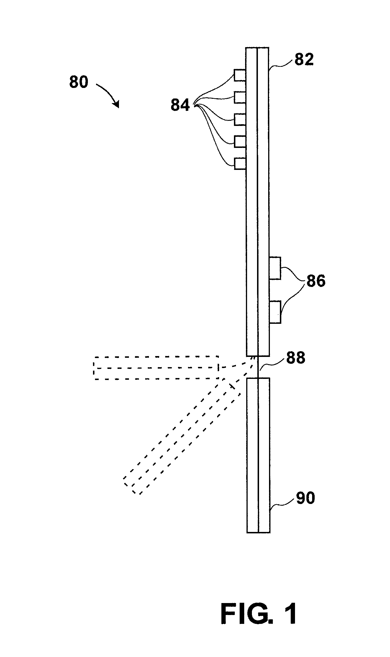
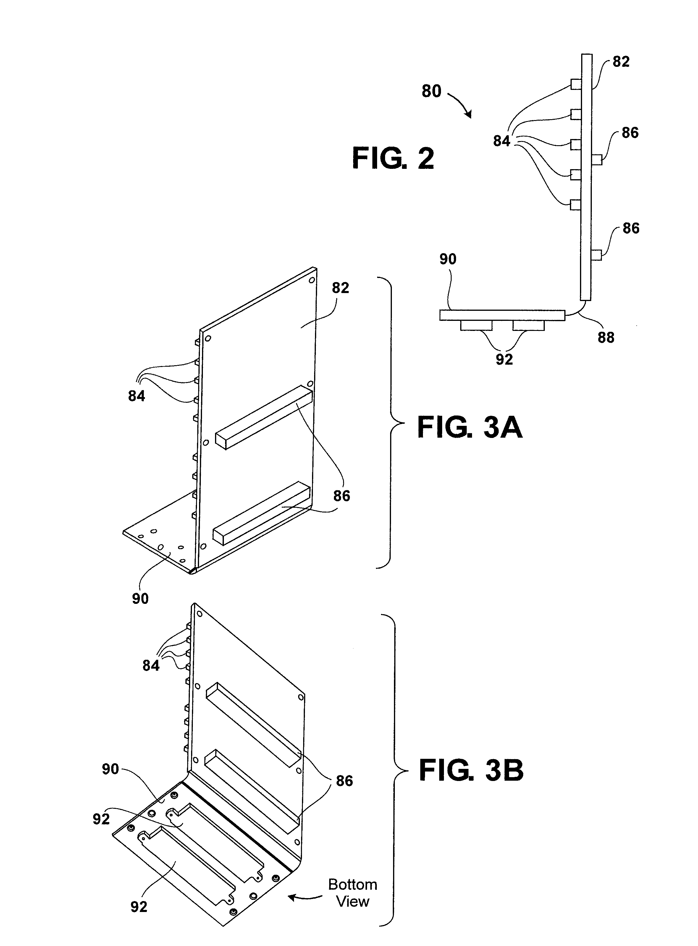
[0025]An invention for an apparatus for a low-cost semiconductor test interface system is disclosed. In the following description, numerous specific details are discussed in order to provide a thorough understanding of the present invention. In one embodiment of the invention, a module board for the test head of a device test system is provided to enable designing a low-cost, extendable and mechanically efficient test head.

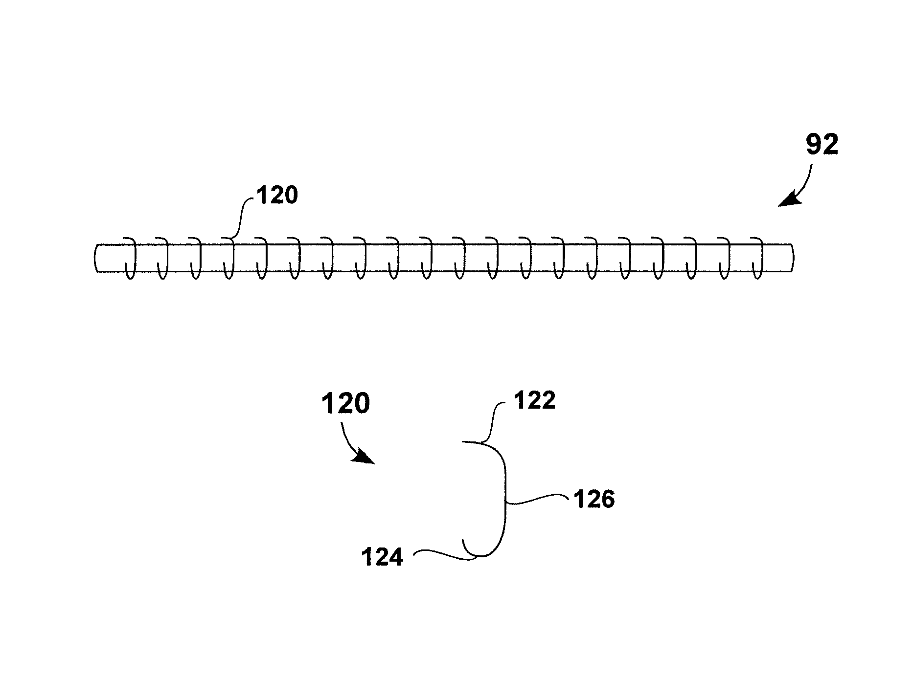
[0026]The module board is designed to remove mechanical inefficiencies of commercially available pogo pin test boards. The pogo pin connectors include thin and long substantially straight metallic pins (or connector wires) projected out of the pogo pin connector base block. The pogo pin connectors are expensive and have a short life span due to frequent pin bending and breakages. Replacing these connectors results in reduced overall efficiency. Furthermore, because test signals sent from a test analyzer to a device under test have to travel comparatively long dist...


PUM


Abstract

A system for testing a device under test (DUT), in which electrical coupling among a module board, a low profile connector, and, a DIB is established by applying a pressure on the module board toward the DUT, is provided. The system includes a test head bracket secured inside a test head, the test head bracket includes the module board having a first section including a plurality of connectors to couple a test analyzer to the module board, a second section including a plurality of contacts pads to electrically couple the module board to the DUT, and, a flexible board to enable the first section to be placed at an angle with respect to the second section. The test head bracket also includes a module board stiffener mechanically securing the first section and the second section to the test head and the low profile connector electrically couples the module board to the DUT.

Description

CROSS REFERENCE TO RELATED APPLICATION[0001]This application is a divisional of U.S. Ser. No. 11 / 941,034, filed Nov. 15, 2007, now U.S. Pat. No. 7,768,280, which is incorporated herein by reference in its entirety.BACKGROUND OF THE INVENTION[0002]Testing is a critical activity in semiconductor device manufacturing, including probe and assembly operations. The manufacturing environment at the testing stage is characterized by multiple products, test equipment with varying capability, and specialized kits and handlers that may be product and equipment specific.[0003]Currently available commercial test-interface systems are incapable of being quickly adapted for testing of different types of devices and consequently do not allow for expanded testing of the device under test. Moreover, commercial test-interface systems are not capable, without being substantially modified, of testing both digital and analog devices. Furthermore, the mechanical design of commercial test-interface systems...

Claims


Application Information

Patent Timeline
Patent Type & Authority Patents(United States)
IPC IPC(8): G01R31/20
CPCG01R31/2889
Inventor WRIGHT, ADAM J.FOERSTEL, JOSEPH W.BANKE, MARK ANDREWITO, KEN A.
Owner ALTERA CORP
Why Eureka
Try Eureka