
Solid-state imaging device with charge transfer transistor on different substrates

a charge transfer transistor and solid-state imaging technology, applied in the field of solid-state imaging devices, can solve the problems of serious disadvantages in the increase of chip size due to the increase of chip size, and achieve the effects of reducing the size of electronic devices, reducing chip size, and reducing chip siz

Active Publication Date: 2014-07-29
SONY CORP
View PDF34 Cites 23 Cited by
  • Summary
  • Abstract
  • Description
  • Claims
  • Application Information

AI Technical Summary

Benefits of technology

The patent text describes a way to make a camera sensor that is smaller and less expensive. This can result in smaller and less costly electronic devices that use this sensor.

Problems solved by technology

In the solid-state imaging device market, in which pixels are being refined and increased in number year after year, an increased cost due to the increased chip size is becoming a serious disadvantage.
Another problem with this type of CMOS solid-state imaging devices having the photoelectric converter sections and accumulation capacitor sections formed on the same substrate surface is a limited light receiving area of the photoelectric converter section because the accumulation capacitor sections occupy a significant area on the substrate.

Method used


Image

  • Solid-state imaging device with charge transfer transistor on different substrates
  • Solid-state imaging device with charge transfer transistor on different substrates
  • Solid-state imaging device with charge transfer transistor on different substrates

Examples


embodiment

1. Embodiment

A Solid-State Imaging Device

[1.1 Entire Structure of the Solid-State Imaging Device]

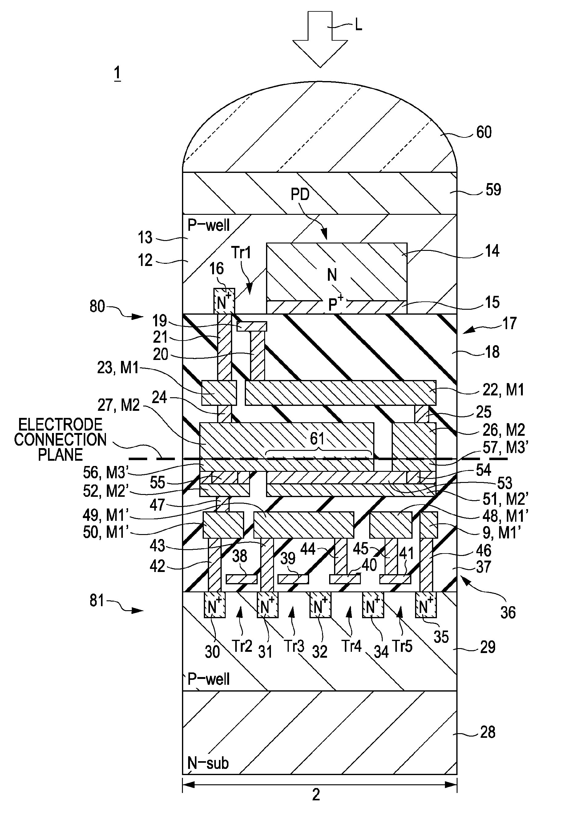
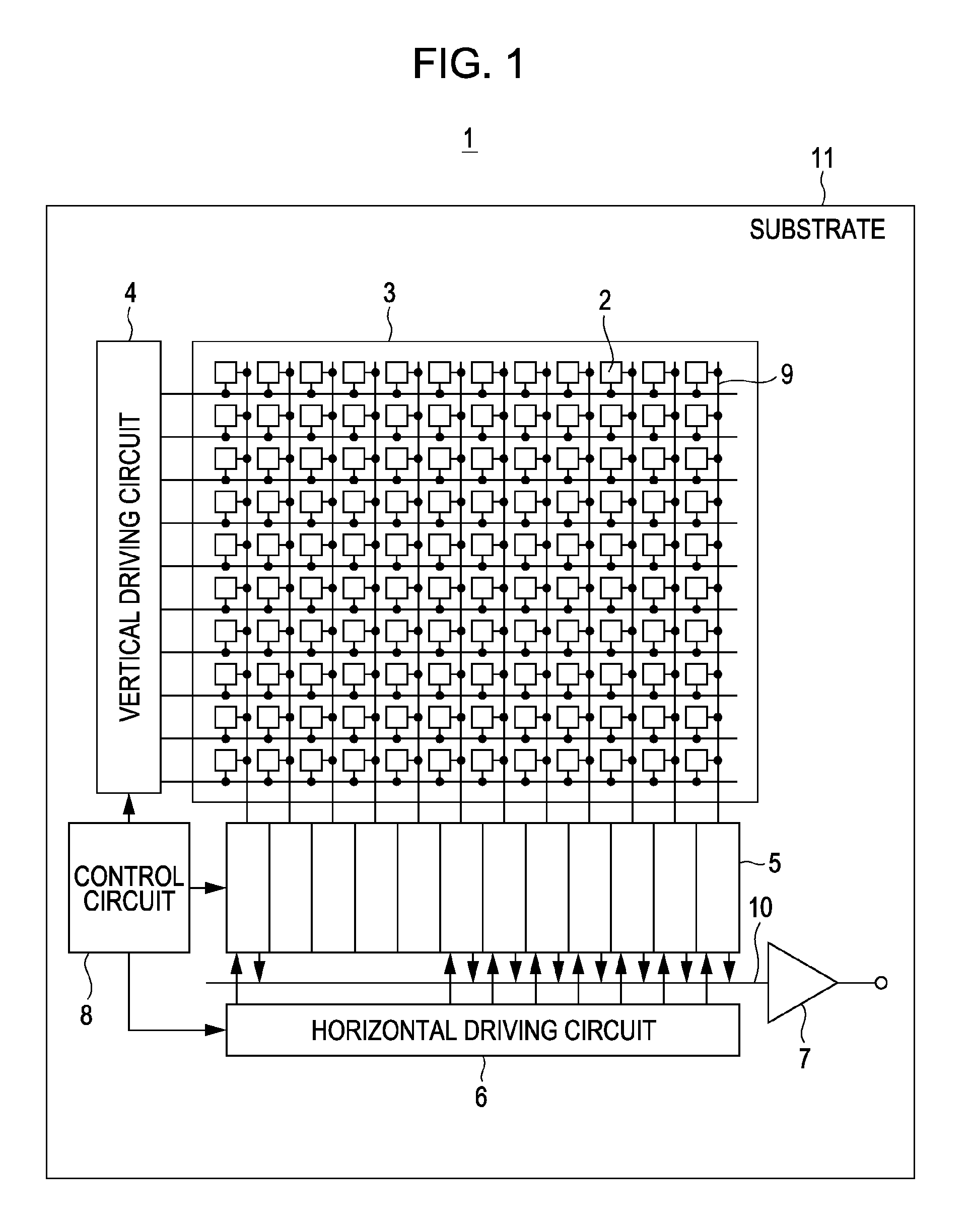
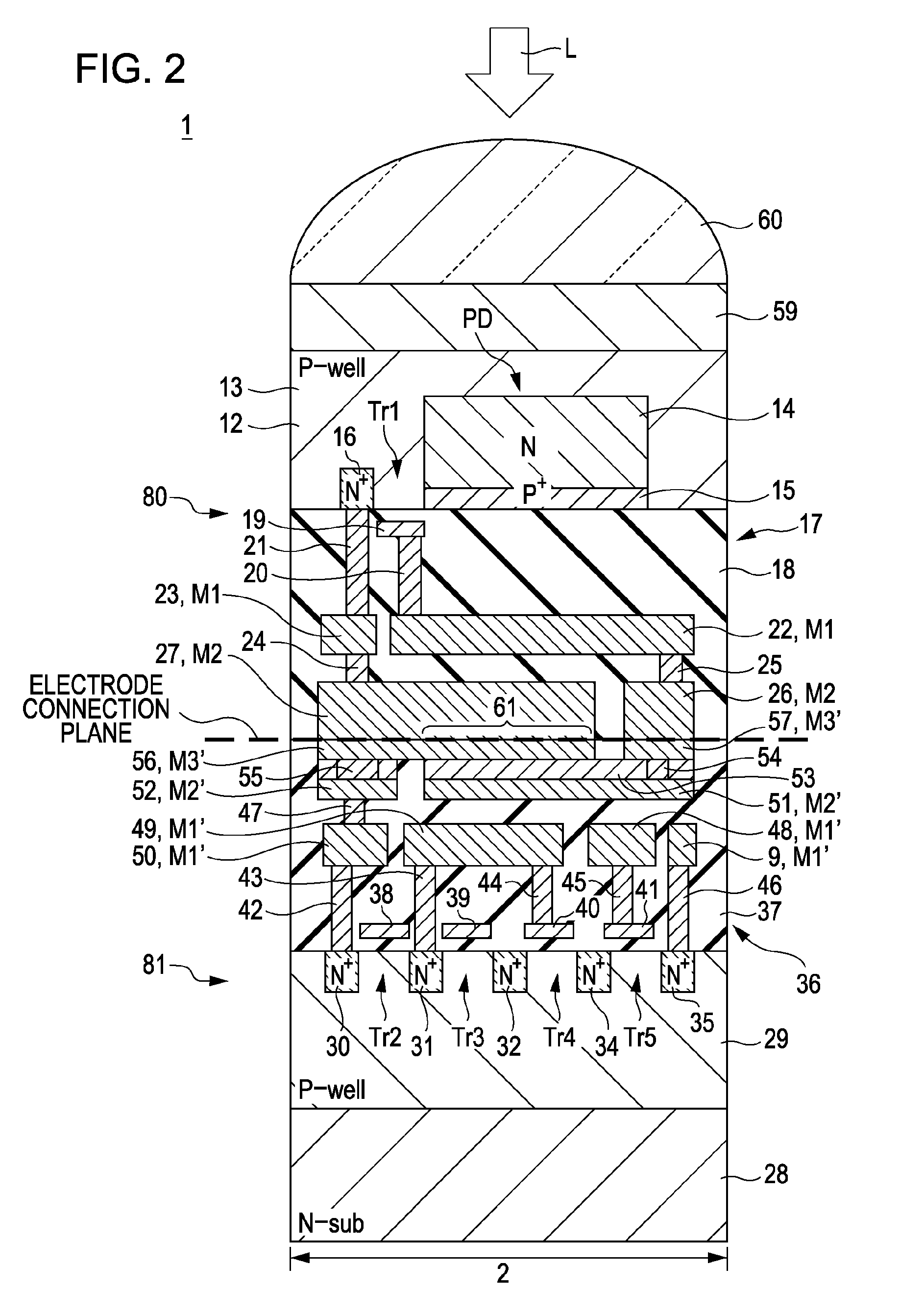
[0039]FIG. 1 schematically shows the entire structure of a solid-state imaging device 1 according to an embodiment of the present invention.

[0040]The solid-state imaging device 1 in the present embodiment has a pixel section 3 including a plurality of pixels 2 arrayed on a silicon substrate 11, a vertical driving circuit 4, a column signal processing circuit 5, a horizontal driving circuit 6, an output circuit 7, and a control circuit 8.

[0041]The plurality of pixels 2, each including a photoelectric converter section made of a photodiode, a charge accumulation capacitor section, and a plurality of MOS transistors, are regularly arranged in a two-dimensional array on the substrate 11. The MOS transistors included in the pixel 2 may be four MOS transistors including a transfer transistor, a reset transistor, a selection transistor, and an amplification transistor, or may be three MOS trans...


PUM


Abstract

A solid-state imaging device includes a plurality of pixels, each of which includes a photoelectric converter section formed on a first substrate to generate and accumulate signal charges corresponding to incident light, a charge accumulation capacitor section formed on the first substrate or a second substrate to temporarily hold the signal charges transferred from the photoelectric converter section, and a plurality of MOS transistors formed on the second substrate to transfer the signal charges accumulated in the charge accumulation capacitor section, connection electrodes formed on the first substrate, and connection electrodes formed on the second substrate and electrically connected to the connection electrodes formed on the first substrate.

Description

BACKGROUND OF THE INVENTION[0001]1. Field of the Invention[0002]The present invention relates to a solid-state imaging device, and in particular to a CMOS solid-state imaging device equipped with a global shutter function, as well as to a method of manufacturing the solid-state imaging device. The present invention also relates to a method of driving the solid-state imaging device, as well as to an electronic apparatus in which the solid-state imaging device is employed.[0003]2. Description of the Related Art[0004]In recent years, video cameras and electronic still cameras have been widespread. In these cameras, a charge coupled device (CCD) or amplified solid-state imaging device is employed. In the amplified solid-state imaging device, signal charges generated by and accumulated in the photoelectric converter section in a light receiving pixel are transferred to an amplifier provided in this pixel and an amplified signal is output from the pixel. A plurality of such pixels are arr...

Claims


Application Information

Patent Timeline
Patent Type & Authority Patents(United States)
IPC IPC(8): H01L21/768H04N5/369H04N5/374H01L21/3205H04N5/335H01L27/146H04N3/14H01L23/522H04N25/00
CPCH01L27/148H01L27/14687H01L27/1469H01L2224/80896H01L2924/13091H01L2224/80895H04N5/3591H04N5/353H01L2924/13062H01L27/14636H04N5/37452H01L27/14632H01L27/1464H01L27/14634H01L2224/08121H01L2224/80194H01L2224/08145H01L2224/80357H01L2224/08058H01L2224/08137H04N25/621H04N25/771H01L2924/00H04N25/53
Inventor TAKAHASHI, HIROSHI
Owner SONY CORP
Learn More