Unlock instant, AI-driven research and patent intelligence for your innovation.

Semiconductor device having equalizing circuit equalizing pair of bit lines

a technology of a semiconductor and a bit line, which is applied in the field of semiconductor devices, can solve the problems of increasing not only circuit scale but also power consumption, and requiring a lot of time for equalizing operation,

Active Publication Date: 2014-08-12
LONGITUDE LICENSING LTD
View PDF18 Cites 14 Cited by
  • Summary
  • Abstract
  • Description
  • Claims
  • Application Information

AI Technical Summary

Benefits of technology

This solution enables efficient equalizing operations and synchronized timing adjustments, preventing errors and reducing power consumption by utilizing external potential as an equalizing signal without increasing circuit complexity or power consumption.

Problems solved by technology

Thus, when a pair of bit lines are short-circuited using an equalizing circuit, the gate-source and gate-drain voltages of a transistor constituting the equalizing circuit become small, resulting in much time being required in the equalizing operation.
For example, assuming that the internal potential VPERI is 1.0 V and precharge level VBLP is 0.5 V, the gate-source voltage (VPERI-VBLP) of a transistor constituting the equalizing circuit is 0.5 V. That is, it is difficult to ensure sufficient ON-current.
Using the boost potential poses a problem in increases in not only circuit scale but also power consumption.
As a result, it becomes difficult to adjust a timing between a signal to control a word line, which is controlled by internal potential and thus relatively less influenced by the voltage condition of the external potential VDD, and a equalizing signal.
In some cases, equalizing operation may erroneously start before reset of the word line.

Method used


Image

  • Semiconductor device having equalizing circuit equalizing pair of bit lines
  • Semiconductor device having equalizing circuit equalizing pair of bit lines
  • Semiconductor device having equalizing circuit equalizing pair of bit lines

Examples


Embodiment Construction

[0022]Preferred embodiments of the present invention will be explained below in detail with reference to the accompanying drawings.

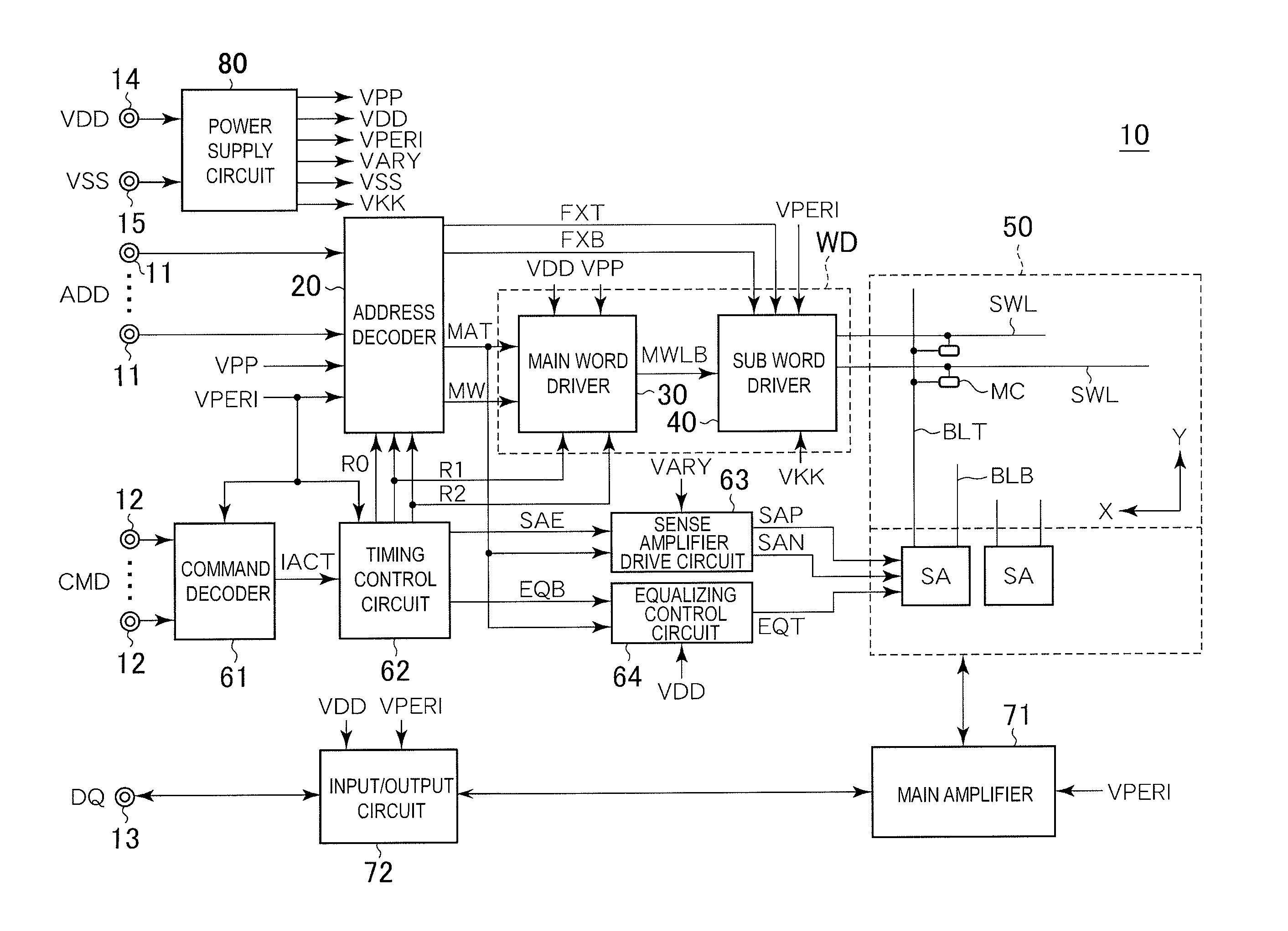
[0023]FIG. 1 is a block diagram illustrating a configuration of a semiconductor device according to a preferred embodiment of the present invention. FIG. 1 mainly illustrates a row system access circuit part, and a column system access circuit part is omitted.

[0024]As illustrated in FIG. 1, a semiconductor device 10 according to the present embodiment has, as external terminals, an address terminal 11, a command terminal 12, a data terminal 13, and power supply terminals 14 and 15.

[0025]The address terminal 11 is a terminal to which an address signal ADD is externally supplied, and the input address signal ADD is supplied to an address decoder 20. The address decoder 20 is a circuit for predecoding the address signal ADD. The address decoder 20 outputs a signal as a result of decoding a part of the address signal ADD as a mat selection signal MAT, output...


PUM


Abstract

A semiconductor device includes: a sense amplifier including an equalizing circuit that equalizes a pair of bit lines; an equalizing control circuit that converts the amplitude of an equalizing signal into a VDD level, and a word driver that controls a sub word line based on a timing signal. The word driver includes a level shift circuit for changing the operation timing of the sub word line in accordance with the VDD level, allowing a timing to complete the equalizing operation and a timing to reset the sub word line to synchronize even when the level of the VDD level is changed.

Description

BACKGROUND OF THE INVENTION[0001]1. Field of the Invention[0002]The present invention relates to a semiconductor device and more particularly relates to a semiconductor device in which an equalizing circuit is provided in a sense amplifier.[0003]2. Description of Related Art[0004]As generally known, data stored in a semiconductor memory device such as a DRAM (Dynamic Random Access Memory) is read by amplifying a potential difference appeared at a pair of bit lines through read operation. To perform sense operation, it is necessary to precharge the pair of bit lines to the same potential and, in general, a bit line driven to high potential (VARY) and a bit line driven to low potential (VSS) are short-circuited using an equalizing circuit to perform the precharge operation. In this case, the precharge level is set to intermediate potential (VBLP) between the VARY and VSS.[0005]In recent years, the internal voltage of a semiconductor device is lowered for reduction of power consumption...

Claims


Application Information

Patent Timeline
Patent Type & Authority Patents(United States)
IPC IPC(8): G11C7/00
CPCG11C11/4091G11C8/08G11C11/4085G11C7/08G11C11/4094G11C8/14
Inventor OKAHIRO, TETSUAKI
Owner LONGITUDE LICENSING LTD