Method for making an integrated circuit substrate having laminated laser-embedded circuit layers

a technology of integrated circuit substrate and laser-embedded circuit layer, which is applied in the direction of printed circuit manufacturing, printed circuit aspects, conductive pattern formation, etc., can solve the problem of substantially higher cost of a typical multi-layer substrate than a single or double-sided circuit substrate, and achieve the effect of increasing the density of interconnection

Active Publication Date: 2014-09-09
AMKOR TECH SINGAPORE HLDG PTE LTD
View PDF180 Cites 14 Cited by
  • Summary
  • Abstract
  • Description
  • Claims
  • Application Information

AI Technical Summary

Benefits of technology

[0007]The above objectives of providing a thin, low-cost multi-layer substrate having increased interconnect density is provided in a substrate having laminated layers including laser-embedded conductive patterns and a method for manufacturing.

Problems solved by technology

However, the cost of a typical multi-layer substrate is substantially higher than a single or double-sided circuit substrate.

Method used


Image

  • Method for making an integrated circuit substrate having laminated laser-embedded circuit layers
  • Method for making an integrated circuit substrate having laminated laser-embedded circuit layers
  • Method for making an integrated circuit substrate having laminated laser-embedded circuit layers

Examples


Embodiment Construction

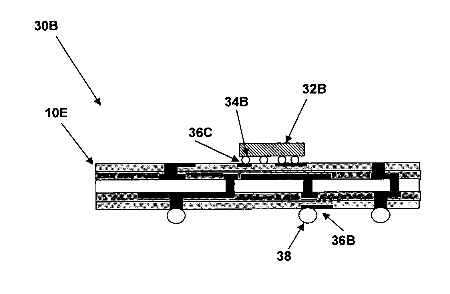
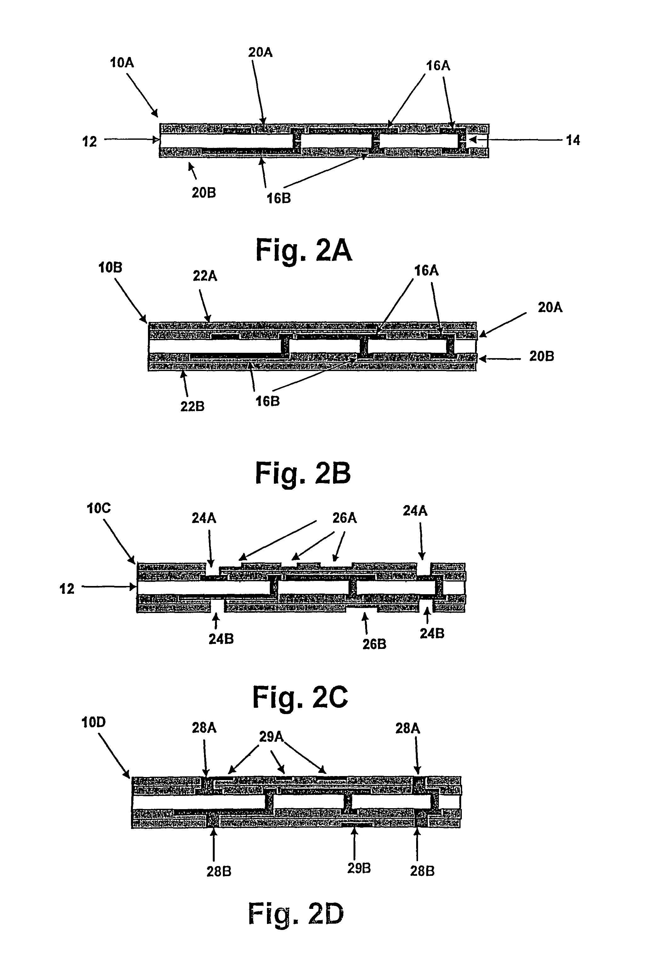
[0014]The above-incorporated patent applications disclose various processes and structures for manufacturing low-cost substrates having high conductor density and electrical integrity by laser-embedding conductive patterns below the surface of a substrate. The present invention transforms a prepared substrate having conductors etched, printed or plated on surfaces thereof into a laminated multi-layer substrate having laser-embedded conductors in the laminated layers. The addition of laser-embedded laminated layers provides a very high conductor density, while adding a low incremental cost to a low-cost substrate.

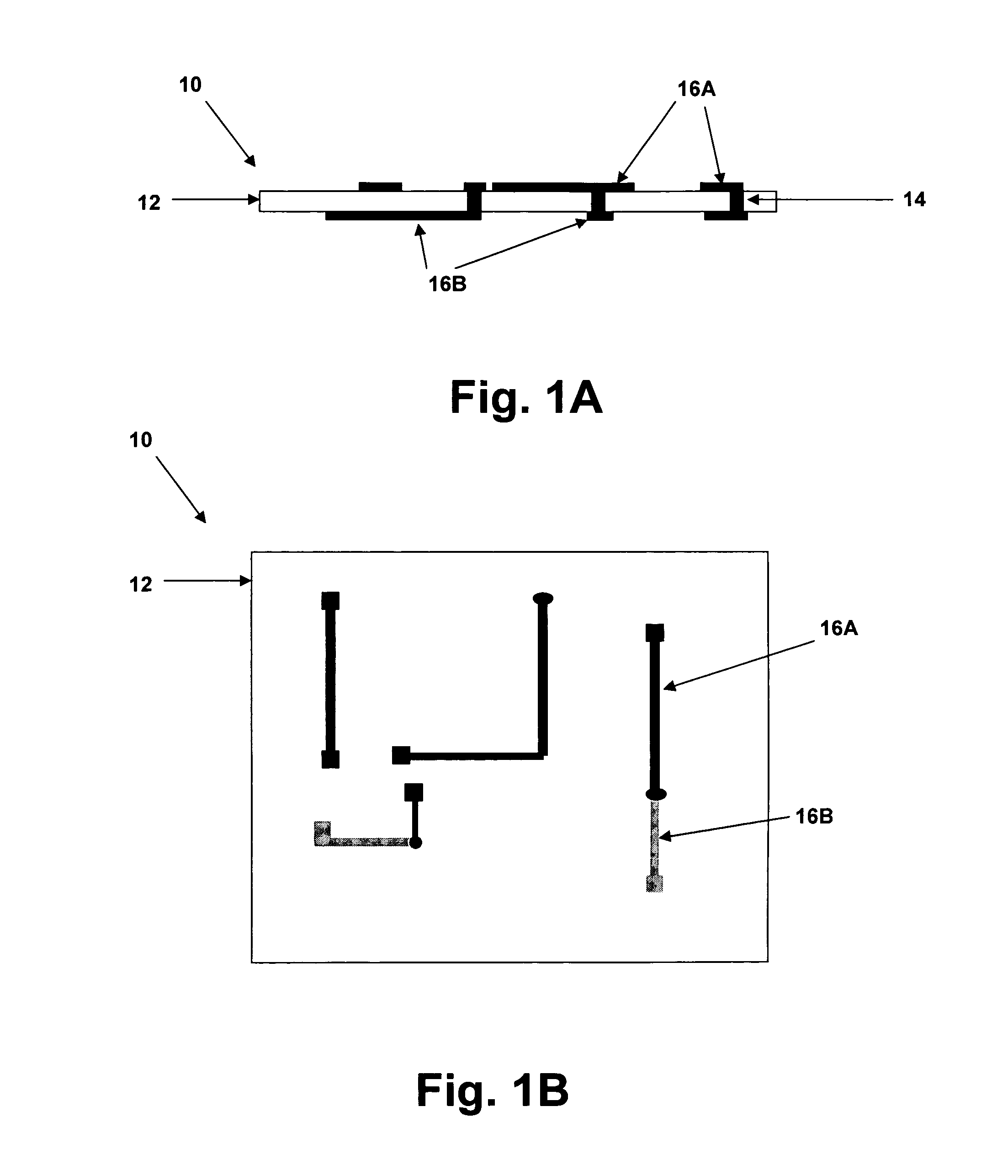
[0015]Referring now to the figures and in particular to FIG. 1A, a side view of prepared substrate 10 for use in forming a laminated substrate in accordance with an embodiment of the present invention is depicted. Circuit patterns are provided on both sides of substrate 10 by metal layers 16A and 16B with via connections 14 providing interconnectivity between metal layers 16...


PUM

PropertyMeasurementUnit
conductiveaaaaaaaaaa
dielectricaaaaaaaaaa
CONDUCTIVEaaaaaaaaaa

Abstract

A method for making an integrated circuit substrate having laminated laser-embedded circuit layers provides a multi-layer high-density mounting and interconnect structure for integrated circuits. A prepared substrate, which may be a rigid double-sided dielectric or film dielectric with conductive patterns plated, etched or printed on one or both sides is laminated with a thin-film dielectric on one or both sides. The thin-film is laser-ablated to form channels and via apertures and conductive material is plated or paste screened into the channels and apertures, forming a conductive interconnect pattern that is isolated by the channel sides and vias through to the conductive patterns on the prepared substrate. An integrated circuit die and external terminals can then be attached to the substrate, providing an integrated circuit having a high-density interconnect.

Description

CROSS-REFERENCE TO RELATED APPLICATIONS[0001]The present application is a divisional of U.S. patent application Ser. No. 10 / 392,738 entitled “INTEGRATED CIRCUIT SUBSTRATE HAVING LAMINATED LASER-EMBEDDED CIRCUIT LAYERS”, now U.S. Pat. No. 6,930,257, issued Aug. 16, 2005, which is a Continuation-in-Part of U.S. patent application entitled “INTEGRATED CIRCUIT SUBSTRATE HAVING LASER-EMBEDDED CONDUCTIVE PATTERNS AND METHOD THEREFOR”, Ser. No. 10 / 138,225 filed May 1, 2002, now U.S. Pat. No. 6,930,256, issued Aug. 16, 2005, by the same inventors and assigned to the same assignee. The above-referenced parent application is also a Continuation-in-Part of U.S. patent application entitled “INTEGRATED CIRCUIT FILM SUBSTRATE HAVING EMBEDDED CONDUCTIVE PATTERNS AND VIAS”, Ser. No. 10 / 261,868 filed Oct. 1, 2002, now abandoned, having at least one common inventor and assigned to the same assignee. The specifications of the above-referenced patent applications are herein incorporated by reference.FI...

Claims


Application Information

Patent Timeline
Patent Type & Authority Patents(United States)
IPC IPC(8): H01R43/00H05K13/00
CPCH05K3/00Y10T29/49169Y10T29/49117H05K2201/0195Y10T29/49126H05K2203/063H05K3/1216H05K3/465Y10T29/49155H05K3/18H05K3/0035H01L2224/16225H01L2224/48091H01L2224/48227H01L2224/48237H01L2924/15311H01L2924/00014
Inventor HINER, DAVID JONHUEMOELLER, RONALD PATRICKRUSLI, SUKIANTO
Owner AMKOR TECH SINGAPORE HLDG PTE LTD
Why Eureka
Try Eureka