Method of manufacturing semiconductor device, substrate processing method, substrate processing apparatus and recording medium
a manufacturing method and semiconductor technology, applied in the direction of liquid surface applicators, coatings, chemical vapor deposition coatings, etc., can solve the problem of difficult to obtain a sic-based film having appropriate characteristics
- Summary
- Abstract
- Description
- Claims
- Application Information
AI Technical Summary
Benefits of technology
Problems solved by technology
Method used
Image

Examples
example 1
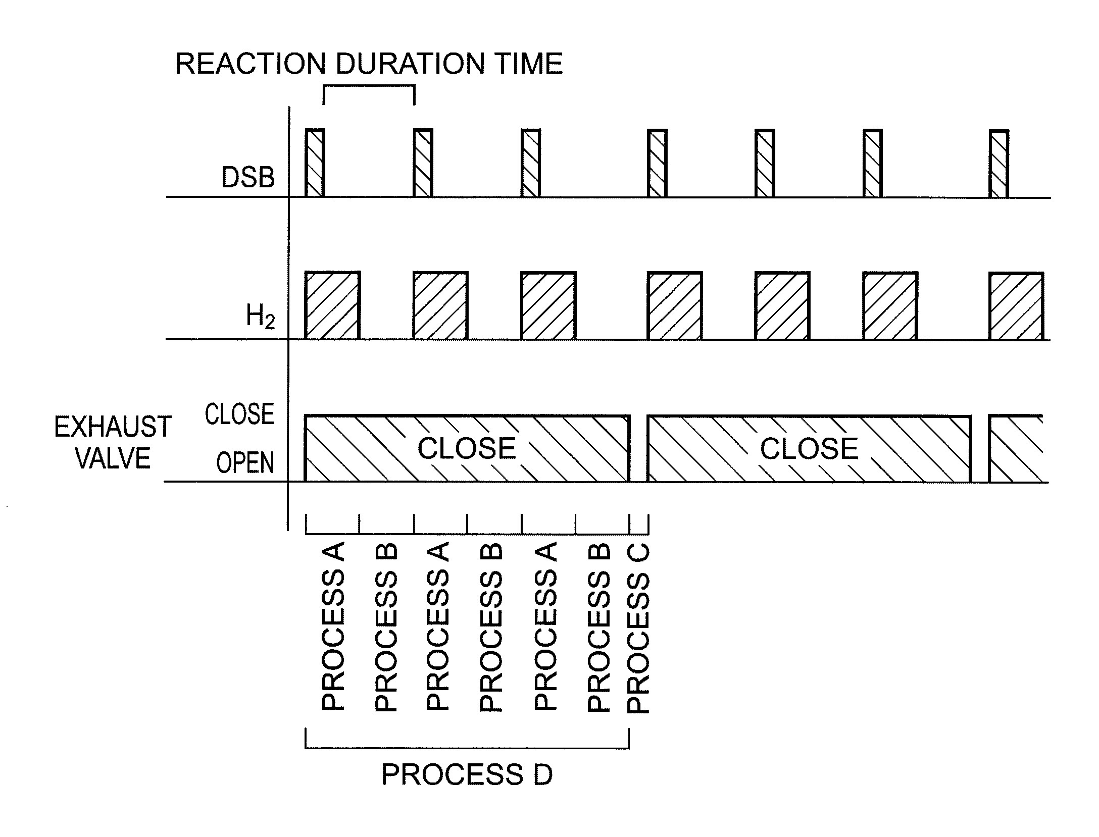
[0152]The SiC film is formed on the wafer 200 as an evaluation sample, by the film forming sequence according to the exemplary embodiment of the invention, described with reference to FIG. 4. Here, the temperatures of the processing chamber 201 and the wafer 200 are set to 425° C., the supply amount of materials, that is, the supply flow rate of the materials and the supply time thereof are respectively set with respect to a volume 100 L of the processing chamber 201 as follows. That is, the supply flow rate and the supply time of the H2 gas are respectively set to 0.20 slm and 40 seconds, and the supply flow rate and the supply time of the DSB gas are respectively set to 0.10 slm and 20 seconds. Other processing conditions in each process are set to conditions within the processing condition range described in the above exemplary embodiment. Further, the concentrations of silicon (Si), carbon (C) and oxygen (O) in the SiC film in the evaluation samples are measured by X-ray Photoel...
example 2
[0155]The SiC film is formed on the wafer 200 having a trench of an aspect ratio of about 4 to 5 on a front surface as an evaluation sample, by the film forming sequence according to the exemplary embodiment of the invention, described with reference to FIG. 4. Here, the temperatures of the processing chamber 201 and the wafer 200 are set to 425° C., the supply amount of materials, that is, the supply flow rate of the materials and the supply time thereof are respectively set with respect to a volume 100 L of the processing chamber 201 as follows. That is, the supply flow rate and the supply time of the H2 gas are respectively set to 0.20 slm and 40 seconds, and the supply flow rate and the supply time of the DSB gas are respectively set to 0.10 slm and 20 seconds. Other processing conditions in each process are set to conditions within the processing condition range described in the above exemplary embodiment. Further, a cross-sectional TEM image of the SiC film in the evaluation s...
example 3
[0157]The SiC film is formed on the wafer 200 as an evaluation sample, by the film forming sequence according to the exemplary embodiment of the invention, described with reference to FIG. 4. Here, processing conditions in each process are set to conditions within the processing condition range described in the above exemplary embodiment. Further, as the evaluation sample, the same evaluation sample as in Example 1 is prepared. With respect to the SiC film in the evaluation sample, a wet etching evaluation using 1% HF solution is performed. As a result, it is confirmed that resistance having a wet etching rate of 1 Å / min or lower is obtained.
PUM
| Property | Measurement | Unit |
|---|---|---|
| temperature | aaaaa | aaaaa |
| pressure | aaaaa | aaaaa |
| time | aaaaa | aaaaa |
Abstract
Description
Claims
Application Information