Distortion tolerant processing

a technology of distortion tolerance and integrated circuit, which is applied in the direction of sustainable manufacturing/processing, semiconductor/solid-state device details, instruments, etc., can solve the problems of slow processing speed, inapplicability to features that are not applicable, and limited step-and-repeat methods, etc., to achieve good device operation, reduce the effect of mask size and low throughpu

Inactive Publication Date: 2014-10-14
FLEHKSENEHBL LTD
View PDF16 Cites 0 Cited by
  • Summary
  • Abstract
  • Description
  • Claims
  • Application Information

AI Technical Summary

Benefits of technology

[0012]The present invention concerns imaging at speed, and as a result, small mask sizes may be used and the throughput is not affected. The linear distortion tolerance may be up to ˜2000 ppm or more because the mask is allowed to overlap on each field, and no adjustment of the magnification is required, as the mask is small enough that lateral mask placement adjustment is sufficient to give good device operation. This makes the process faster, since adjusting the magnification of the image at each site is time consuming, and cannot be done at speed.
[0013]In the present invention, there are no concerns about choosing a magnification to suit the difference in distortion in each axis due to the fact that no adjustment of the magnification of the lens is required. The mask location is shifted and a small mask size is used, which is apt for the current process as the imaging occurs on the fly and at speed with the use a pulsed laser beam.

Problems solved by technology

This step-and-repeat method is limited to patterning of periodic patterns that repeat themselves over a certain period, such as the patterns required for defining an active-matrix array of TFTs in a display.
However, one drawback of this approach is that it is not applicable to features that are not periodic such as the interconnect patterns, alignment marks, bonding pads and tab out patterns on the edge of a display.
This makes the process faster, since adjusting the magnification of the image at each site is time consuming, and cannot be done at speed.

Method used


Image

  • Distortion tolerant processing
  • Distortion tolerant processing
  • Distortion tolerant processing

Examples


example

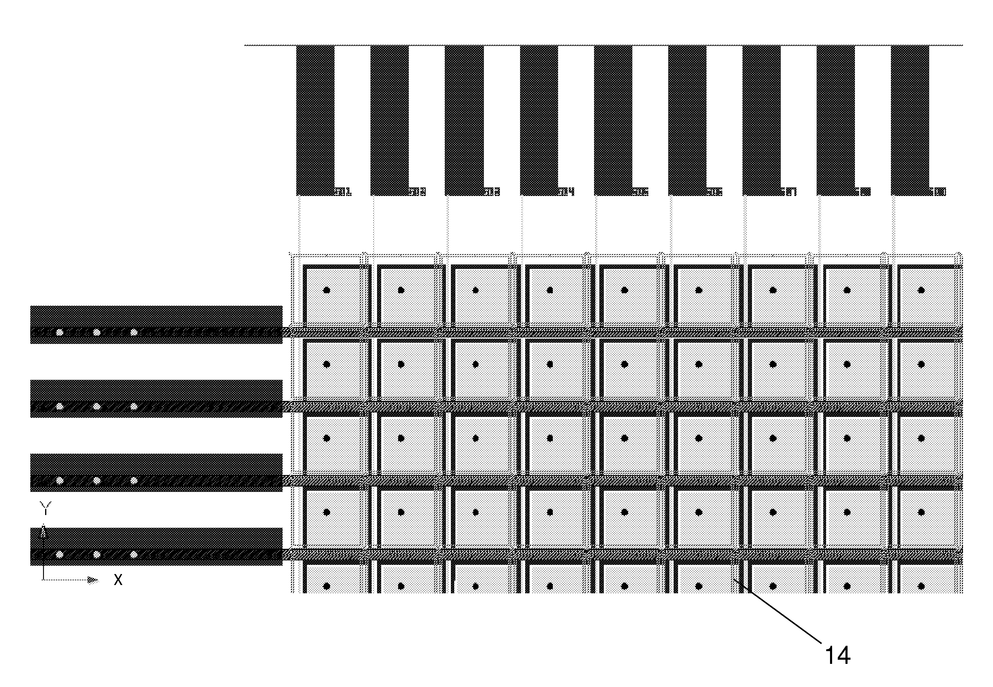
[0051]A low cost method of processing an active-matrix display with top-gate TFT architecture containing non-repetitive patterns on a distorted flexible substrate.

[0052]In the case of an active matrix display with top-gate TFT architecture the non-repetitive pattern to be placed on the lower layer contains interconnects that link the data lines on the source-drain level as well as gate interconnect lines to the row-and-column driver chips or the flexible connectors mounted on the edge of the display, as well as non-periodic alignment marks and test structures.

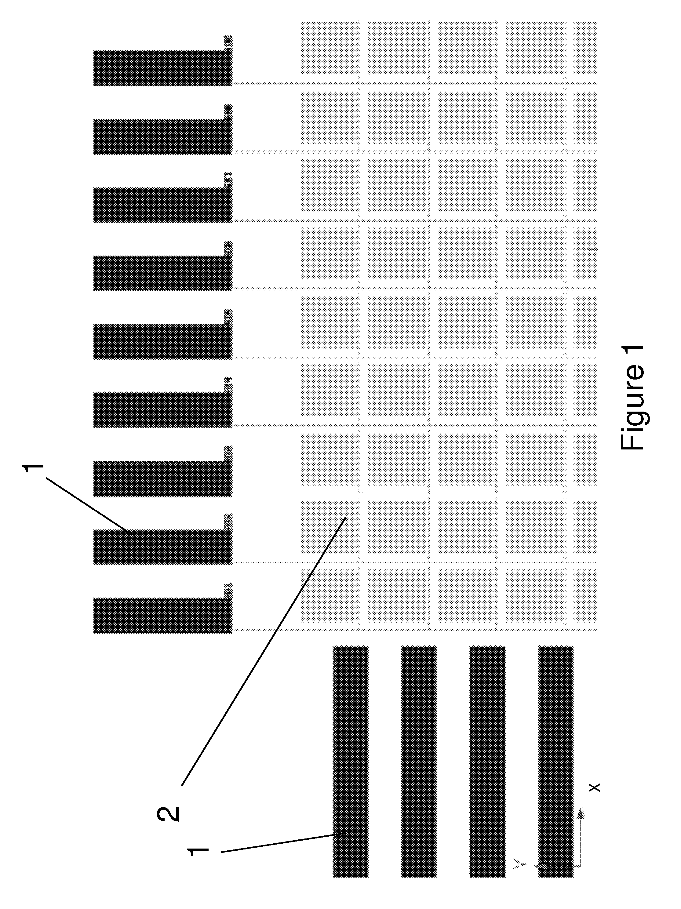
[0053]These non-repetitive patterns on the lower layer can be integrated together with periodic patterns such as the source-drain of the active matrix array while the gate electrodes and gate interconnects, semiconducting active layer island, common electrode structures, and any pixel electrode patterns need to be laid out as periodic patterns on an upper layer. Particularly accurate relative alignment is required between the l...


PUM

PropertyMeasurementUnit
temperatureaaaaaaaaaa
thicknessaaaaaaaaaa
thicknessaaaaaaaaaa

Abstract

A method of manufacturing an integrated circuit (IC) for driving a flexible display includes depositing a pattern of spatially non-repetitive features in a first layer on a flexible substrate, said pattern of spatially non-repetitive features not substantially regularly repeating in both of two orthogonal directions (x,y) in the plane of the substrate; depositing a pattern of spatially repetitive features in a second layer on said first layer; aligning said second layer and said first layer so as to allow electrical coupling between said non-repetitive features and said repetitive features, wherein distortion compensation is applied during deposition of said repetitive features to enable said alignment.

Description

CROSS-REFERENCE TO RELATED APPLICATIONS[0001]This application is the U.S. National Phase under 35 U.S.C. §371 of International Application No. PCT / GB2007 / 050599, filed Oct. 1, 2007, designating the United States and published in English on Apr. 10, 2008, as WO 2008 / 041027, which claims priority to United Kingdom Application No. 0619548.1, filed Oct. 3, 2006 and United Kingdom Application No. 0716608.5, filed Aug. 28, 2007.FIELD OF THE INVENTION[0002]The present invention relates to a distortion-tolerant method of processing an integrated circuit, incorporating a flexible substrate or a substrate that is susceptible to distortion.DESCRIPTION OF RELATED ART[0003]A route for achieving more cost-effective electronics such as large-area displays and RFID circuits at higher throughputs than are available using conventional inorganic semiconductor processing is required within organic electronics. In order to achieve devices such as large area displays and high-speed logic circuits, conduc...

Claims


Application Information

Patent Timeline
Patent Type & Authority Patents(United States)
IPC IPC(8): H01L33/00G03F7/20H01L51/00H01L51/05
CPCG03F7/70791H01L51/0018H01L51/0541H01L27/283H01L27/124H01L51/0097Y02E10/549Y02P70/50H10K71/233H10K71/60H10K77/111H10K10/464H10K19/10
Inventor HAYTON, CARLCAIN, PAUL A.
Owner FLEHKSENEHBL LTD
Why Eureka
Try Eureka