
Distortion tolerant processing
a technology of distortion tolerance and processing method, applied in the direction of sustainable manufacturing/processing, instruments, final product manufacturing, etc., can solve the problems of slow processing speed, inapplicability to features that are not applicable, and limited step-and-repeat methods, etc., to achieve good device operation, reduce the effect of mask size and reduce the effect of throughpu
- Summary
- Abstract
- Description
- Claims
- Application Information
AI Technical Summary
Benefits of technology
Problems solved by technology
Method used
Image

Examples
Embodiment Construction
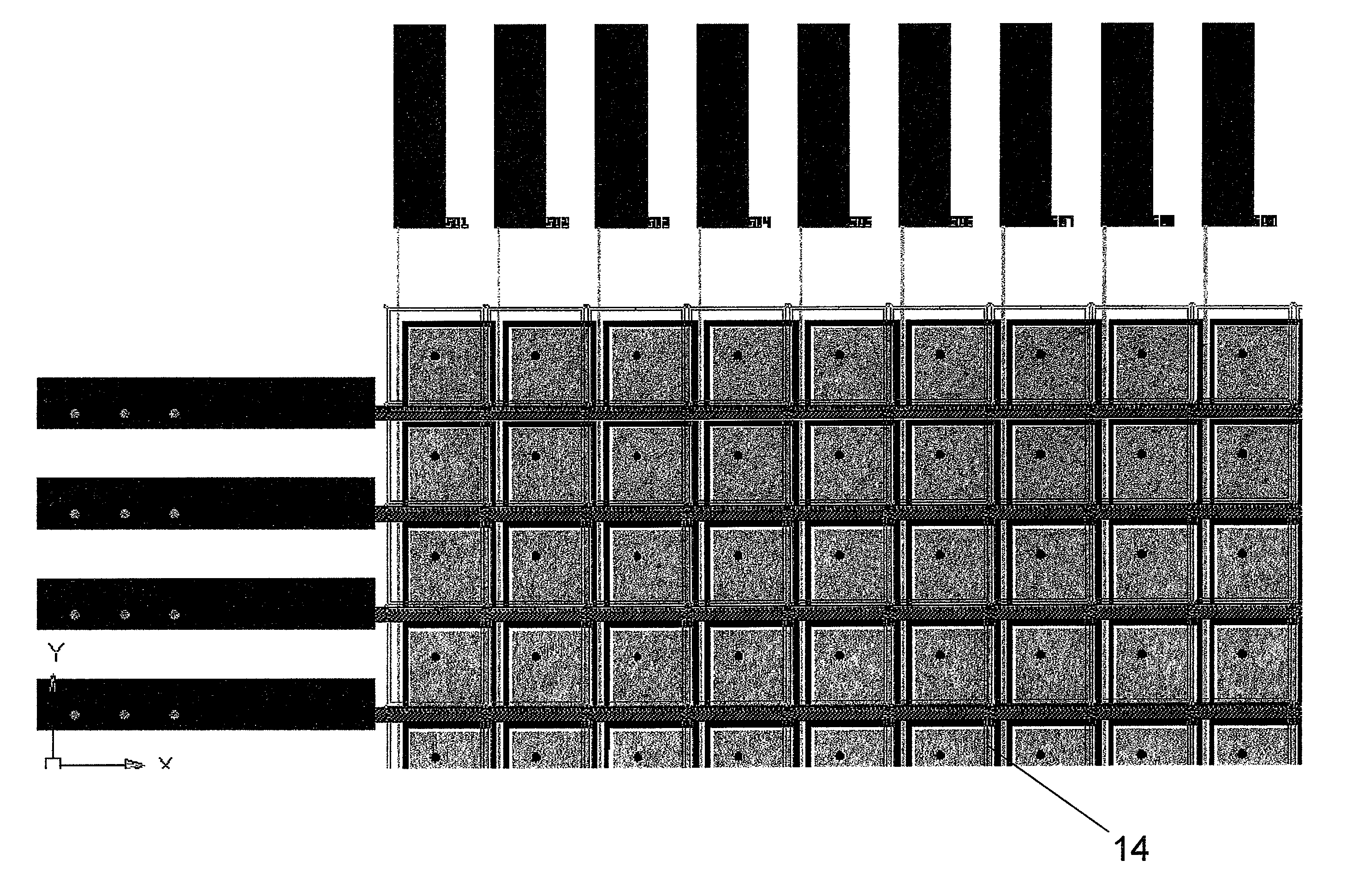
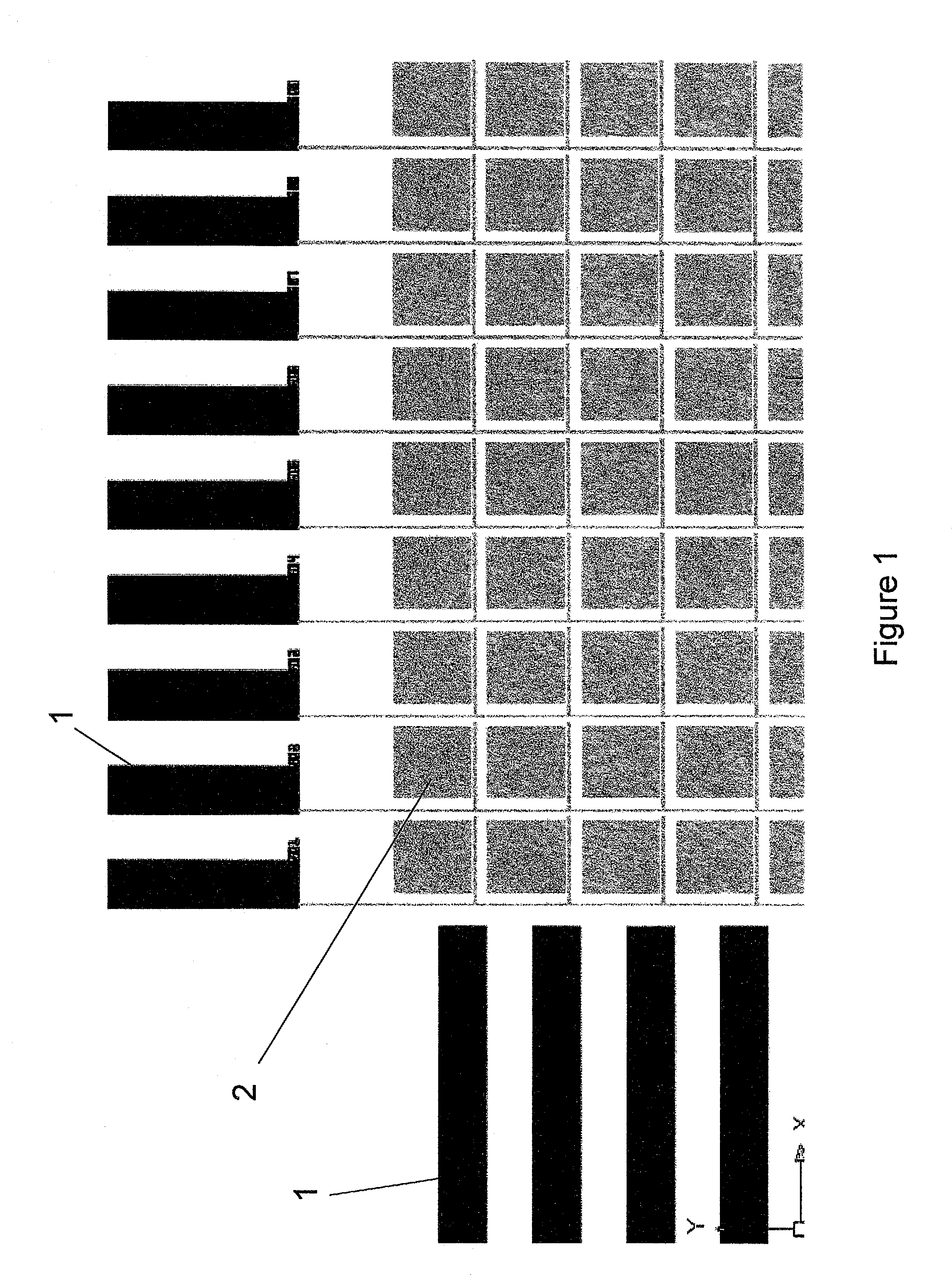
[0051]Example: A low cost method of processing an active-matrix display with top-gate TFT architecture containing non-repetitive patterns on a distorted flexible substrate.
[0052]In the case of an active matrix display with top-gate TFT architecture the non-repetitive pattern to be placed on the lower layer contains interconnects that link the data lines on the source-drain level as well as gate interconnect lines to the row-and-column driver chips or the flexible connectors mounted on the edge of the display, as well as non-periodic alignment marks and test structures.
[0053]These non-repetitive patterns on the lower layer can be integrated together with periodic patterns such as the source-drain of the active matrix array while the gate electrodes and gate interconnects, semiconducting active layer island, common electrode structures, and any pixel electrode patterns need to be laid out as periodic patterns on an upper layer. Particularly accurate relative alignment is required betw...
PUM
| Property | Measurement | Unit |
|---|---|---|
| temperature | aaaaa | aaaaa |
| thickness | aaaaa | aaaaa |
| thickness | aaaaa | aaaaa |
Abstract
Description
Claims
Application Information