Semiconductor light emitting device

a technology of light-emitting devices and semiconductors, which is applied in the manufacture of semiconductor/solid-state devices, semiconductor devices, electrical devices, etc., can solve the problems of wasting acceptable regions, generating more likely defective regions, and reducing so as to improve light extraction efficiency, shorten the average distance traveled, and reduce the number of reflections of light

Active Publication Date: 2014-11-04
NICHIA CORP
View PDF37 Cites 3 Cited by
  • Summary
  • Abstract
  • Description
  • Claims
  • Application Information

AI Technical Summary

Benefits of technology

[0010]Accordingly, an object of the present invention is to provide a semiconductor light emitting device using a large-sized laminated semiconductor light emitting element which has improved light extraction efficiency, and a manufacturing method thereof.
[0013]In the semiconductor light emitting device of the present invention, the division of the semiconductor laminate into the semiconductor regions can shorten the average distance traveled by the light emitted from the active layer until it reaches the sides. This can decrease the number of reflection of the light inside the semiconductor laminate, thus improving the light extraction efficiency. The width of the trench is smaller than the average particle diameter of the fluorescent particle, which can suppress the deposition of the fluorescent particles inside the trenches when manufacturing the semiconductor light emitting device. Thus, the light extraction efficiency can be improved.
[0014]According to the manufacturing method of the present invention, the width of the trench is smaller than the average particle diameter of the fluorescent particle, which can suppress the deposition of the fluorescent particles inside the trenches in the covering step. Thus, the semiconductor light emitting device with improved light extraction efficiency can be manufactured.
[0015]In the semiconductor light emitting device of the present invention, the fluorescent particles are less likely to be deposited inside the trenches. The present invention provides the semiconductor light emitting device using the large-sized laminated semiconductor light emitting element with the improved light extraction efficiency. The manufacturing method of the present invention can manufacture the semiconductor light emitting device using the large-sized laminated semiconductor light emitting element with improved light extraction efficiency.

Problems solved by technology

However, when the size of the semiconductor light emitting element is increased, a defective region is more likely to be generated in a semiconductor laminate of the element.
Therefore, the number of good large-sized semiconductor light emitting elements that can be formed from one piece of wafer is decreased, which results in poor yield.
Further, the acceptable regions are disadvantageously wasted.
In this case, the fluorescent particles may enter a gap between the small-sized elements and interrupt the light emitted from the gap.
As a result, light extraction efficiency may be deteriorated.
One problem caused by increasing the size of a semiconductor light emitting element is a reduction in efficiency of light extraction.

Method used


Image

  • Semiconductor light emitting device
  • Semiconductor light emitting device
  • Semiconductor light emitting device

Examples


first embodiment

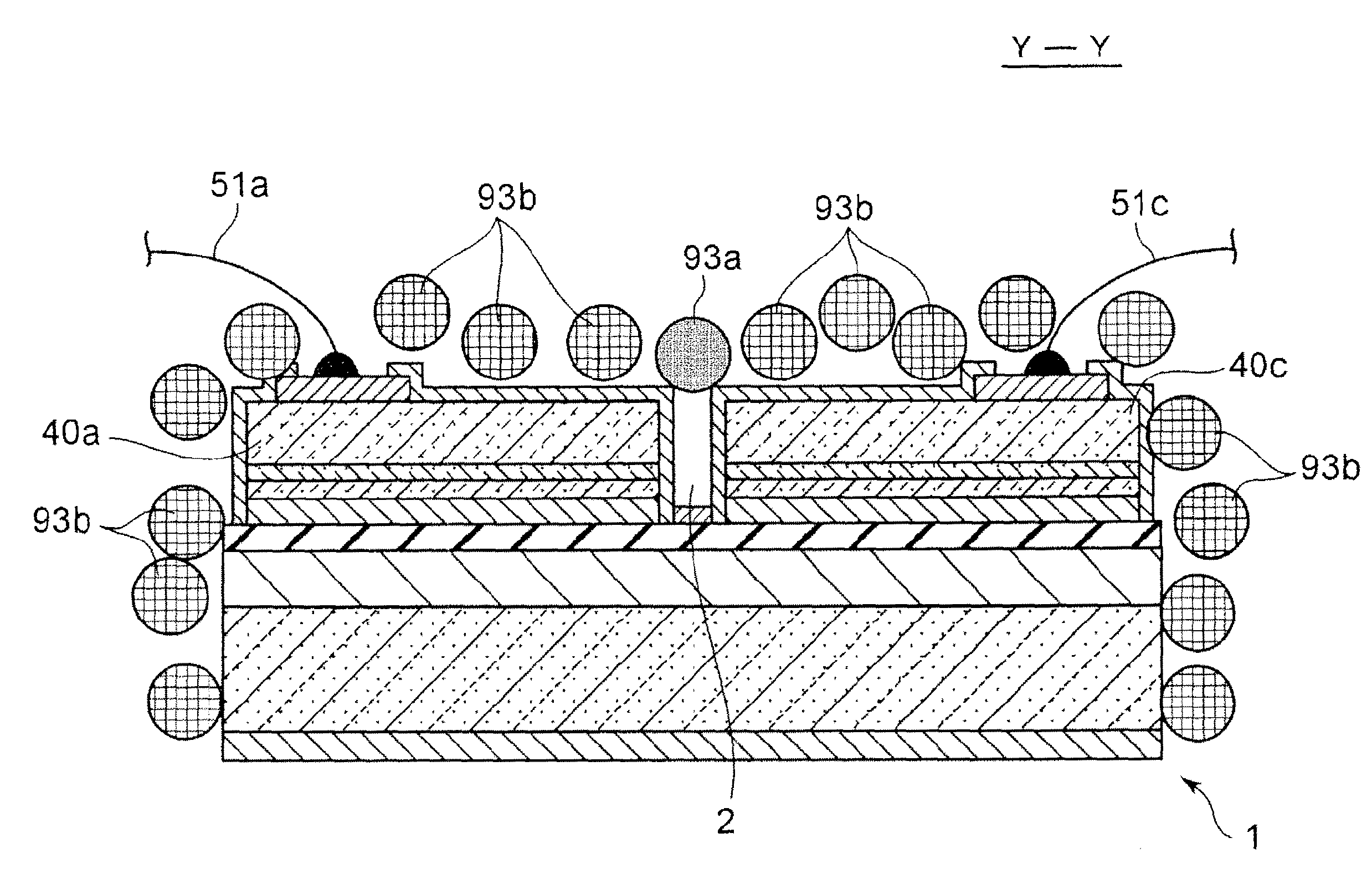
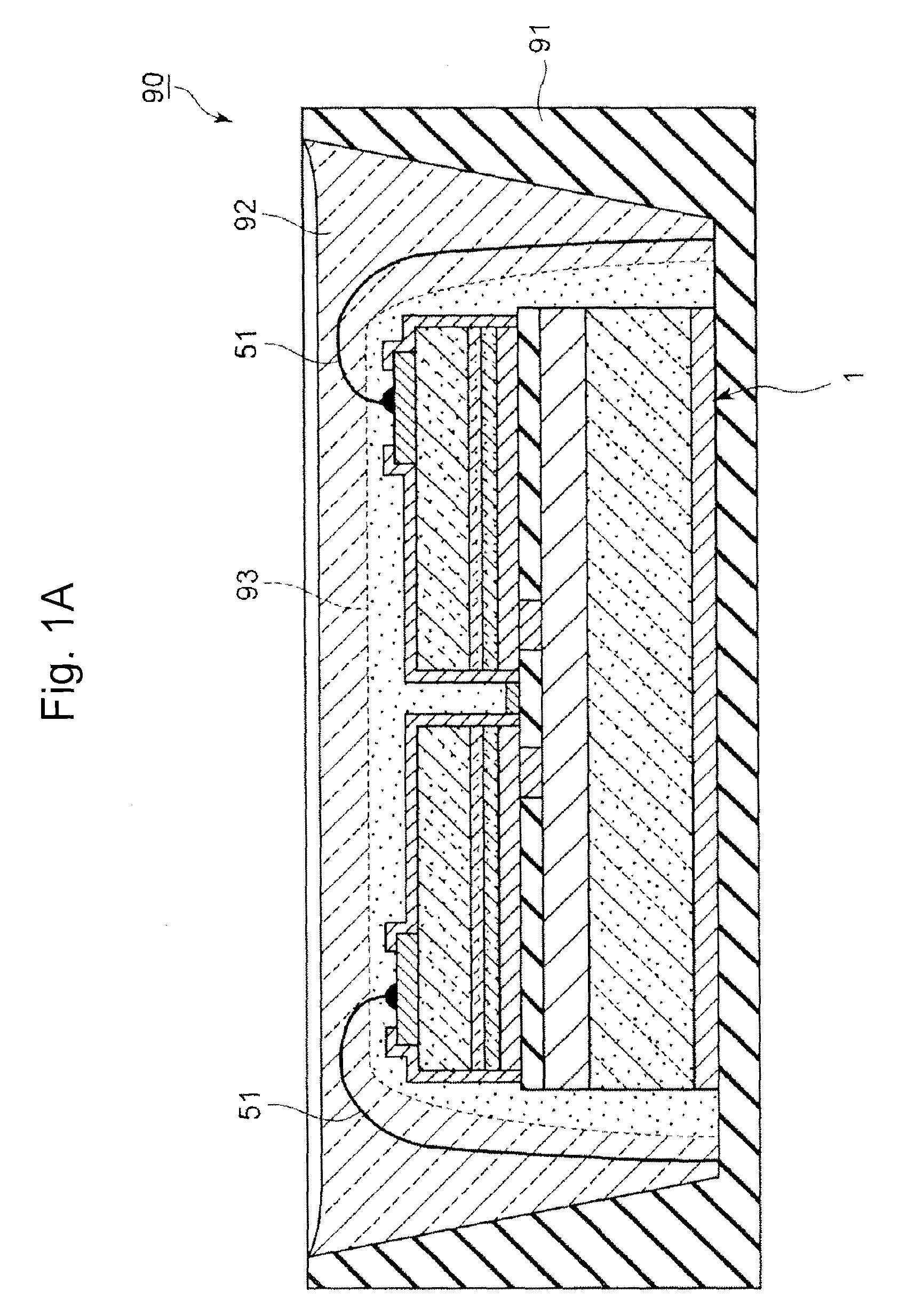
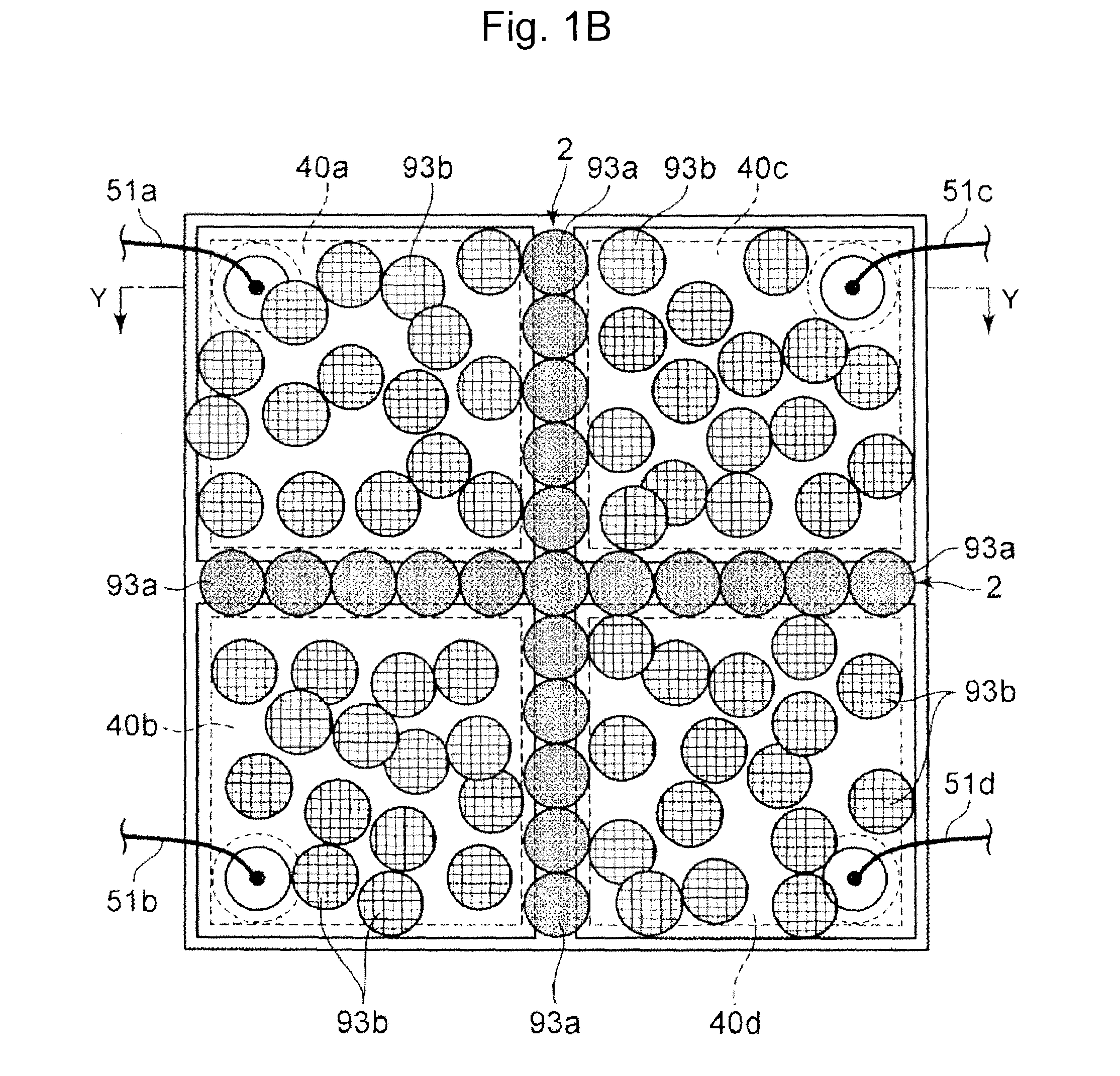
[0061]FIGS. 1A to 1C illustrate a semiconductor light emitting device 90 of the present embodiment. The semiconductor light emitting device 90 includes a semiconductor light emitting element 1 mounted in a recess of a housing 91, and a transparent sealing resin 92 covering the semiconductor light emitting element 1. The transparent sealing resin 92 contains fluorescent particles 93 (i.e., “first fluorescent particles”), and is deposited around the semiconductor light emitting element 1. While the fluorescent particles 93 are depicted as spherical particles in FIGS. 1B and 1C, the fluorescent particles 93 are not necessarily spherical. For example, the fluorescent particles 93 may be irregularly shaped. Regardless of its shape, each of the fluorescent particles has an individual average particle diameter.

[0062]FIGS. 2A and 2B illustrate the semiconductor light emitting element 1. The semiconductor light emitting element 1 includes a junction layer 20, a protective film 80, a reflecti...

second embodiment

[0126]The present embodiment differs from the first embodiment in that the reflection layer 30 is formed up to the bottom 2b of the trench 2 (see FIG. 8). When the reflection 30 is formed of material or the like that is unlikely to migrate, the present modified embodiment is preferable. The reflection layer 30 whose reflectivity is generally higher than that of a dielectric multilayered film allows the light directed toward the bottom 2b of the trench 2 to be effectively reflected and emitted toward the outside of the trench 2. Thus, the formation of the reflection layer 30 up to the bottom 2b of the trench 2 can further improve the light extraction efficiency of the semiconductor light emitting element 1.

[0127]When manufacturing the semiconductor light emitting element 1 of the present embodiment, “(8) region separation step (see FIG. 5I)” of the manufacturing method disclosed in the first embodiment is modified. Specifically, when the trench 2 is formed in the semiconductor lamina...

third embodiment

[0128]The present embodiment differs from the first embodiment in that only the protective film 80 is provided between the support substrate and the semiconductor laminate without providing the reflection layer 30 (see FIG. 9). In the same manner as in the first embodiment, the protective film 80 can also be provided at the bottom 2b of the trench 2. When the material for the reflection layer 30 is likely to migrate, or when the reflection layer 30 is disadvantageously likely to diffuse into the semiconductor laminate 40, the reflection layer 30 is preferably not formed. The formation of the protective film 80 using a dielectric multilayered film instead of the reflection layer 30 permits the light to be reflected from the semiconductor laminate 40 toward the support substrate 10 and thus can suppress the absorption of the light. The inclusion of the protective film 80 formed of the dielectric multilayered film can keep the intensity of light transmitted through the semiconductor la...


PUM


Abstract

A semiconductor light emitting device comprises a semiconductor light emitting element comprising a semiconductor laminate including a p-type semiconductor layer, an active layer and an n-type semiconductor layer which are sequentially laminated, and a conductive support substrate joined to the p-type semiconductor layer side of the semiconductor laminate. The semiconductor laminate is divided into at least two semiconductor regions by a trench. The semiconductor light emitting device further comprises a first transparent sealing resin covering at least a portion of the semiconductor light emitting element, the first transparent sealing resin comprising a plurality of first fluorescent particles, each of the first fluorescent particles having an individual average particle diameter. A width of the trench is smaller than an overall average of the individual average particle diameters of the first fluorescent particles.

Description

BACKGROUND OF THE INVENTION[0001]1. Field of the Invention[0002]The present invention relates to a semiconductor light emitting device and a manufacturing method thereof, and more particularly to a semiconductor light emitting device including a combination of a semiconductor light emitting element and a fluorescent material for wavelength conversion.[0003]2. Description of the Related Art[0004]In recent years, an increase in the size of semiconductor light emitting elements has been required. However, when the size of the semiconductor light emitting element is increased, a defective region is more likely to be generated in a semiconductor laminate of the element. A semiconductor light emitting element having a defective region in a part of the semiconductor laminate is determined to be defective, even when most of the regions in the semiconductor laminate are acceptable. Therefore, the number of good large-sized semiconductor light emitting elements that can be formed from one pie...

Claims


Application Information

Patent Timeline
Patent Type & Authority Patents(United States)
IPC IPC(8): H01L27/15H01L33/40H01L33/00H01L33/50
CPCH01L27/156H01L33/50H01L33/505H01L33/405H01L2224/48091H01L2924/0002H01L2224/73265H01L2933/0016H01L2224/48465H01L33/508H01L2933/0041H01L2924/00014H01L2924/00H01L33/08H01L33/20
Inventor UBAHARA, NOBUHIRODEGUCHI, KOUICHIROHYAMADA, TAKAO
Owner NICHIA CORP
Why Eureka
Try Eureka