Semiconductor devices and methods of manufacturing the same

a technology of semiconductor devices and semiconductors, applied in the direction of semiconductor devices, electrical apparatus, transistors, etc., can solve the problems of difficult control of electrical characteristics between a many defects may be formed at the interface between the group iii-v material and si, and the inability to further improve the performance and integration degree of si-based semiconductor devices in the near future. , to achieve the effect of reducing growth defects and excellent electrical characteristics

Active Publication Date: 2014-12-02
SAMSUNG ELECTRONICS CO LTD
View PDF14 Cites 3 Cited by
  • Summary
  • Abstract
  • Description
  • Claims
  • Application Information

AI Technical Summary

Benefits of technology

[0008]Provided are semiconductor devices with reduced growth defects and excellent electrical characteristics.
[0009]Provided are semiconductor devices with reduced leakage current and excellent operating characteristics.

Problems solved by technology

However, due to limitations in material properties of Si and manufacturing processes, it may become difficult to further improve performance and integration degree of Si-based semiconductor devices in the near future.
However, because there are significant differences between lattice constants and thermal expansion coefficients of a Group III-V material and Si, and surface polarity of the Group III-V material also differs from that of Si, many defects may be formed at an interface between the Group III-V material and Si.
Furthermore, it may be difficult to control electrical characteristics between a Group III-V material and Si.
Therefore, application of a Group III-V material to a Si substrate or a Si-based device may be limited.

Method used


Image

  • Semiconductor devices and methods of manufacturing the same
  • Semiconductor devices and methods of manufacturing the same
  • Semiconductor devices and methods of manufacturing the same

Examples


Embodiment Construction

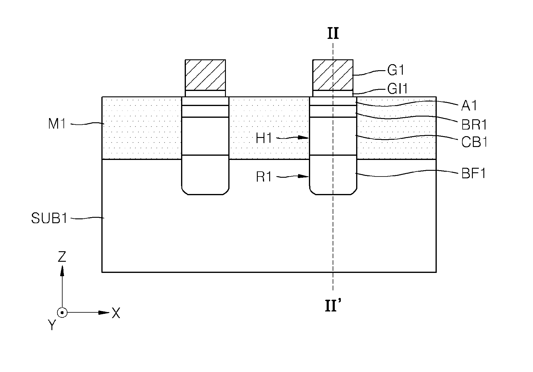
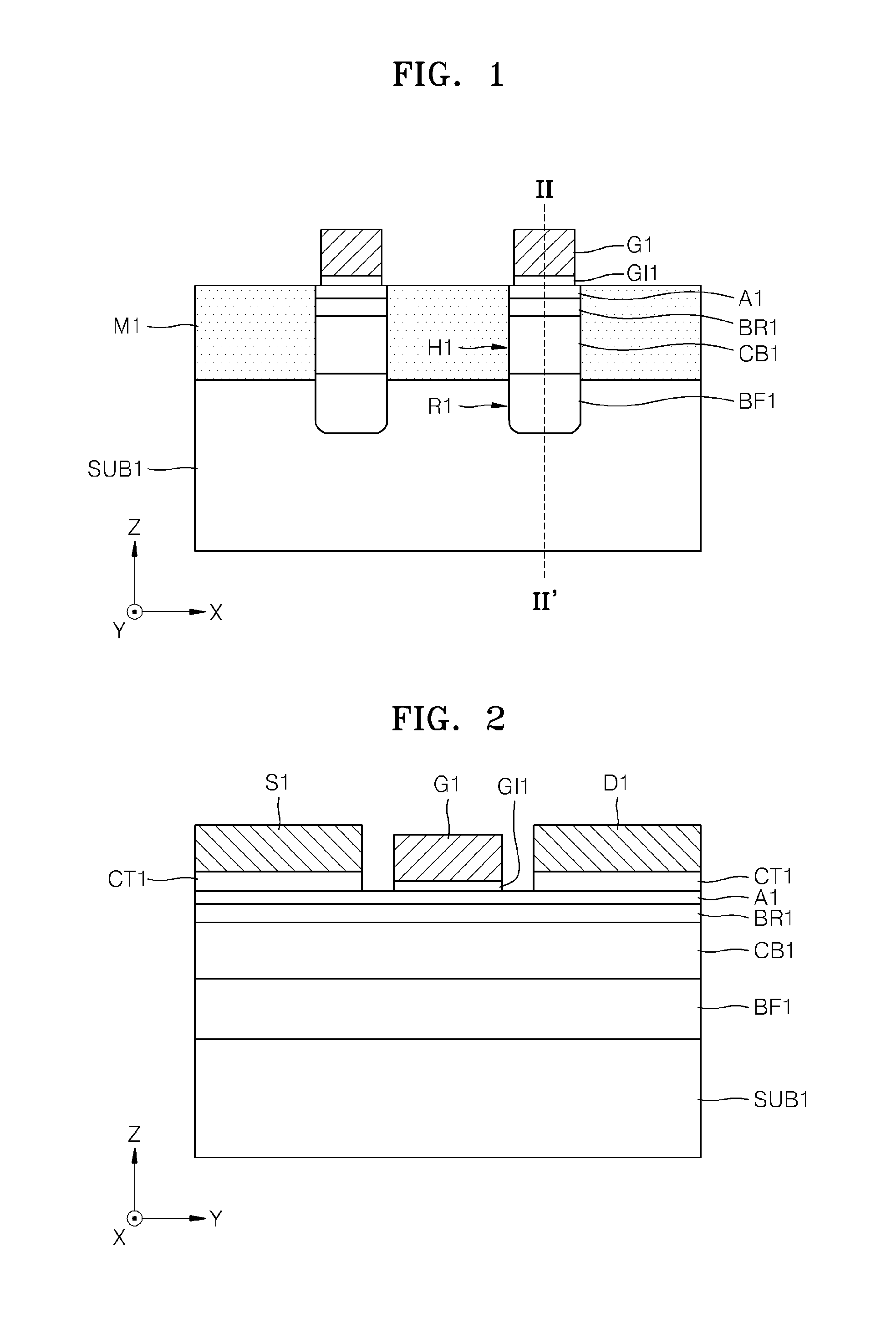
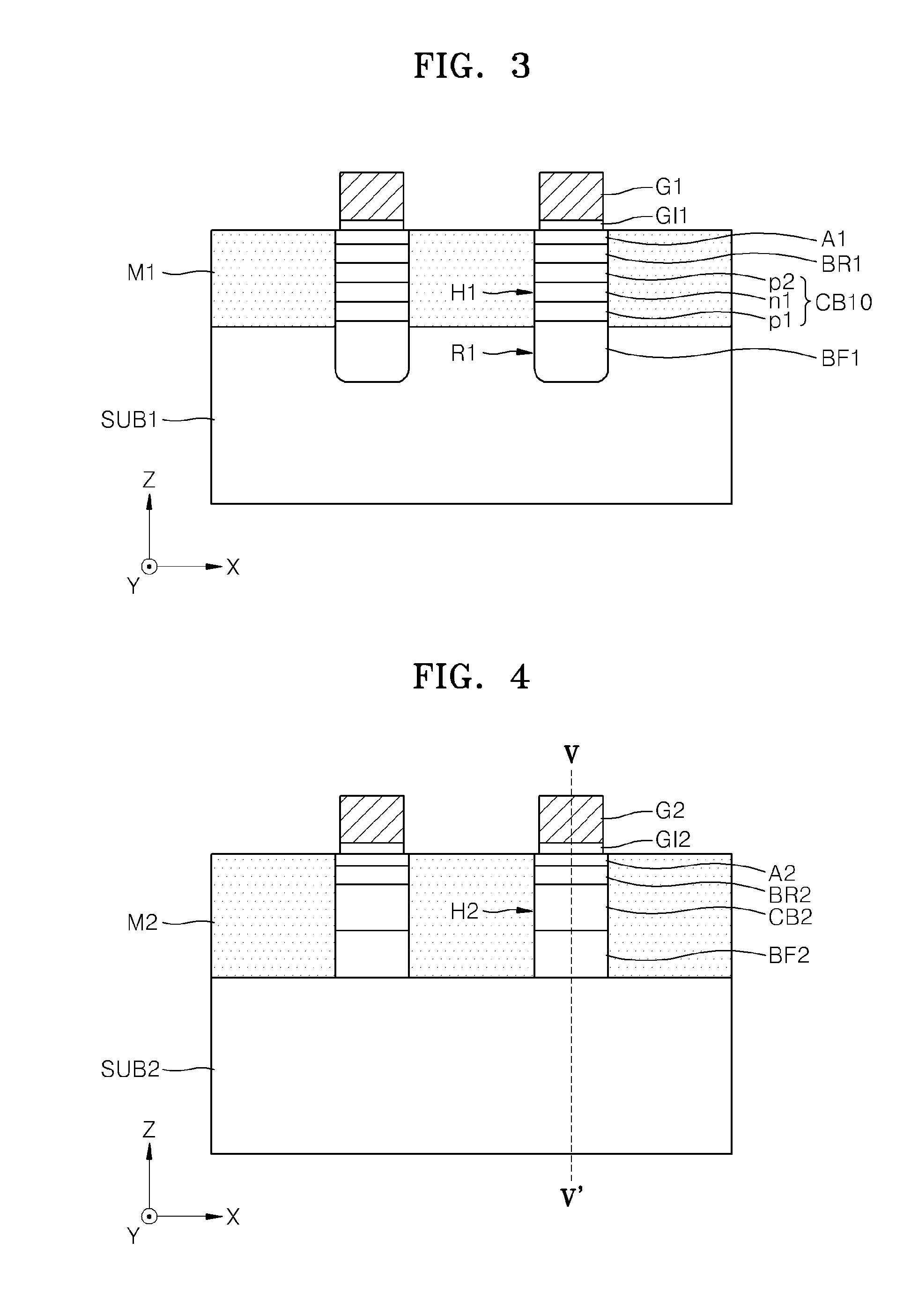
[0068]Various example embodiments will now be described more fully with reference to the accompanying drawings in which example embodiments are shown.

[0069]It will be understood that when an element is referred to as being “connected” or “coupled” to another element, it can be directly connected or coupled to the other element or intervening elements may be present. In contrast, when an element is referred to as being “directly connected” or “directly coupled” to another element, there are no intervening elements present. As used herein the term “and / or” includes any and all combinations of one or more of the associated listed items.

[0070]It will be understood that, although the terms “first”, “second”, etc. may be used herein to describe various elements, components, regions, layers and / or sections, these elements, components, regions, layers and / or sections should not be limited by these terms. These terms are only used to distinguish one element, component, region, layer or secti...


PUM


Abstract

Semiconductor devices including a substrate (e.g., silicon substrate), a multi-layer structure disposed on a portion of the substrate, and at least one electrode disposed on the multi-layer structure and methods of manufacturing the same are provided. The multi-layer structure may include an active layer containing a Group III-V material and a current blocking layer disposed between the substrate and the active layer. The semiconductor device may further include a buffer layer disposed between the substrate and the active layer. In a case that the substrate is a p-type, the buffer layer may be an n-type material layer and the current blocking layer may be a p-type material layer. The current blocking layer may contain a Group III-V material. A mask layer having an opening may be disposed on the substrate so that the multi-layer structure may be disposed on the portion of the substrate exposed by the opening.

Description

CROSS-REFERENCE TO RELATED APPLICATIONS[0001]This application claims the benefit of Korean Patent Application No. 10-2012-0067302, filed on Jun. 22, 2012, in the Korean Intellectual Property Office, the disclosure of which is incorporated herein in its entirety by reference.BACKGROUND[0002]1. Field[0003]The present disclosure relates to semiconductor devices and methods of manufacturing the same, and more particularly, to semiconductor devices including Group III-V semiconductors and methods of manufacturing the same.[0004]2. Description of the Related Art[0005]Silicon (Si)-based semiconductor devices have been developed to have higher integration density and higher performance. However, due to limitations in material properties of Si and manufacturing processes, it may become difficult to further improve performance and integration degree of Si-based semiconductor devices in the near future.[0006]To overcome limitations of Si-based semiconductor devices, research is being made into...

Claims


Application Information

Patent Timeline
Patent Type & Authority Patents(United States)
IPC IPC(8): H01L31/0336H01L29/10H01L29/778H01L21/00H01L31/072H01L21/337H01L29/51H01L29/66H01L29/15H01L29/06H01L29/12
CPCH01L29/7781H01L29/1075H01L29/66462H01L29/0657H01L29/15H01L29/7783H01L29/517H01L29/78H01L29/205H01L29/1079
Inventor LEE, SANG-MOONCHO, YOUNG-JIN
Owner SAMSUNG ELECTRONICS CO LTD
Why Eureka
Try Eureka