SiOx process chemistry development using microwave plasma CVD

a technology of plasma cvd and process chemistry, which is applied in the direction of chemical vapor deposition coating, coating, coating process, etc., can solve the problems of high deposition temperature of siox /sub>films from sif/sub>4, incompatible with advanced device processing and requiring a low thermal budg

Inactive Publication Date: 2014-12-09
APPLIED MATERIALS INC
View PDF49 Cites 6 Cited by
  • Summary
  • Abstract
  • Description
  • Claims
  • Application Information

AI Technical Summary

Problems solved by technology

However, the explosive behavior of SiH4 and corrosive behavior of SiF4 requires strict control over processing conditions and careful handling of the process effluent.
Furthermore, deposition of SiOx films from SiF4 require high deposition temperatures that are incompatible with advanced device processing requiring a low thermal budget.

Method used


Image

  • SiOx process chemistry development using microwave plasma CVD
  • SiOx process chemistry development using microwave plasma CVD
  • SiOx process chemistry development using microwave plasma CVD

Examples


examples

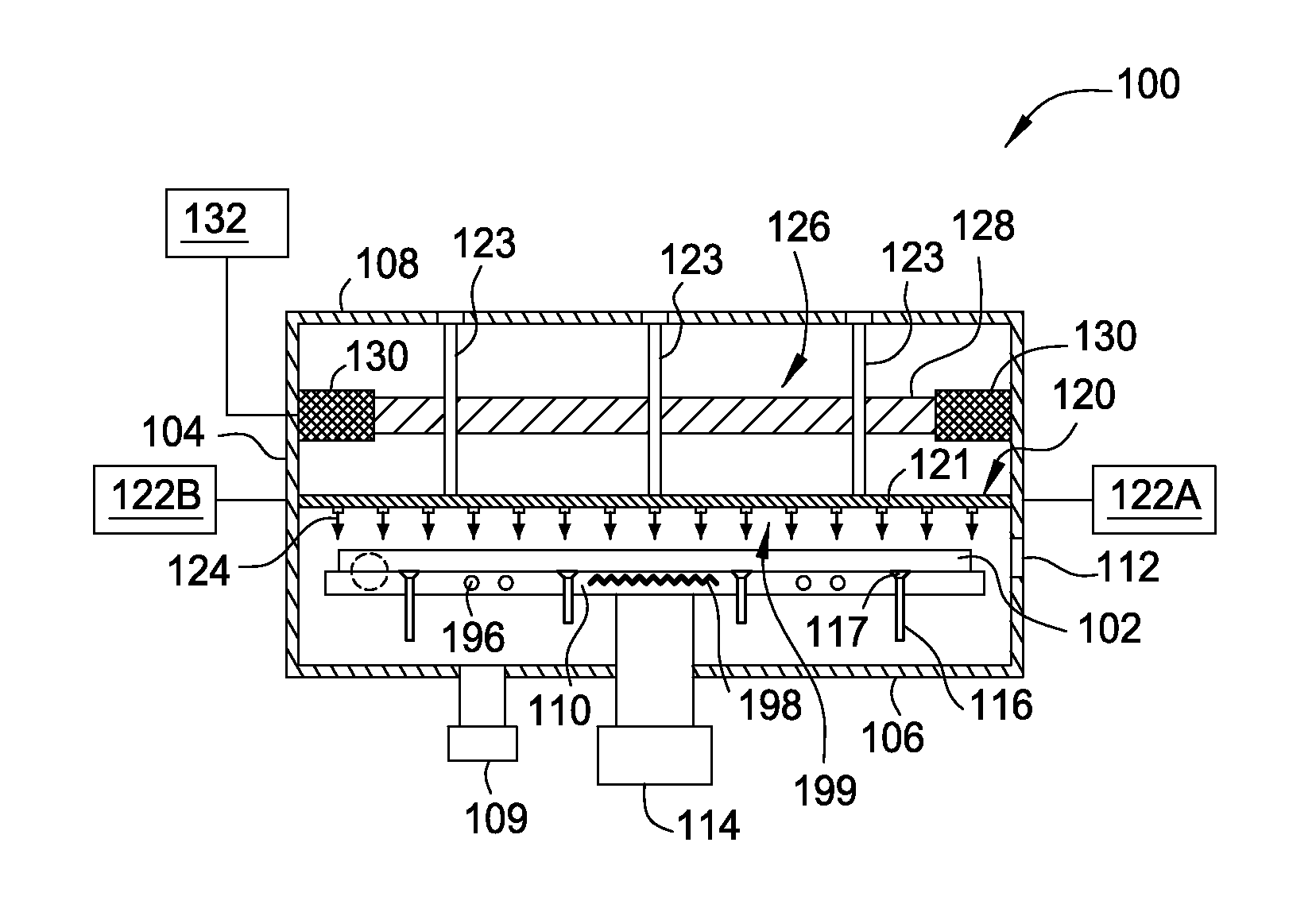
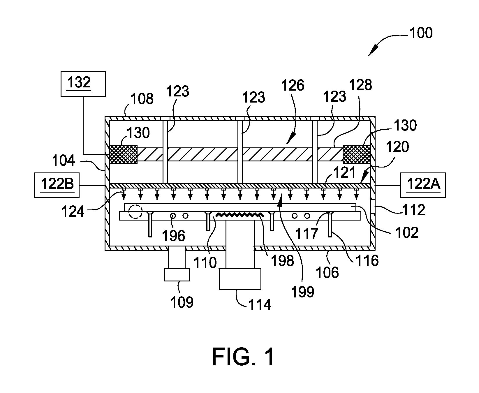
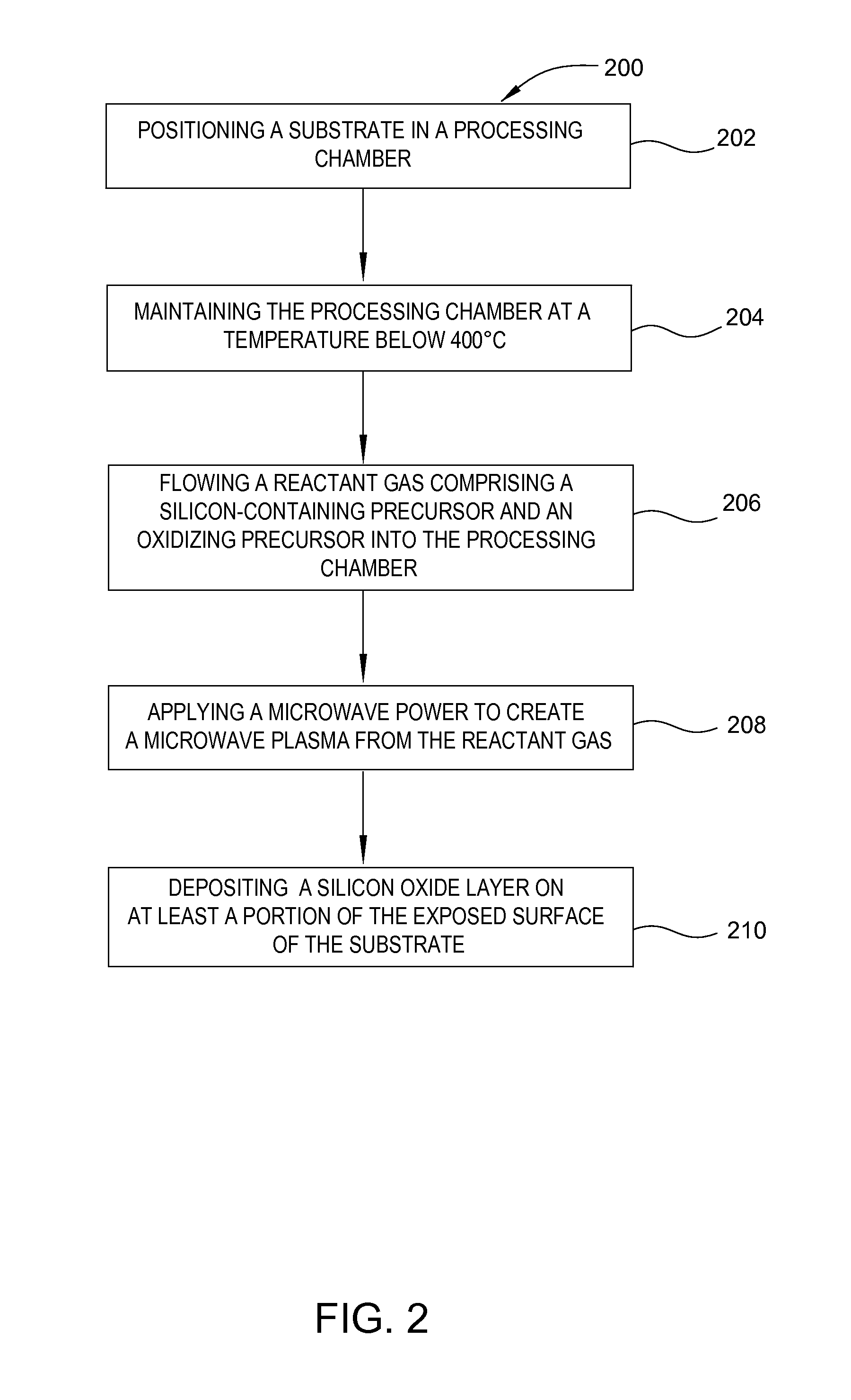
[0055]Described below are examples from experimental data using one or more of the embodiments disclosed previously. Exemplary embodiments described herein are described with reference to an AKT-5500 PX PECVD chamber available from Applied Materials, Inc. located in Santa Clara, Calif. The 5500 PX PECVD chamber is generally is sized to process a substrate having a surface area of 5500 centimeter square. It is to be understood that embodiments described herein can be scaled up or down to compensate for different sized substrates and different sized chambers.

[0056]A first control example shows a range of SiO layer characteristics for layers which were deposited by CCP-PECVD using SiH4 and N2O gases. SiH4 and O2 were not used in CCP-PECVD due to the volatility of the gas combination using CCP plasma. The depositions were performed at 230° C. The flow rate of the SiH4 gas was from 200 sccm to 350 sccm. The flow rate of the N2O gas was from 10000 sccm to 18000 sccm. The capacitive power ...


PUM

PropertyMeasurementUnit
temperatureaaaaaaaaaa

Abstract

Methods for processing a substrate are described herein. Methods can include positioning a substrate in a processing chamber, maintaining the processing chamber at a temperature below 400° C., flowing a reactant gas comprising either a silicon hydride or a silicon halide and an oxidizing precursor into the process chamber, applying a microwave power to create a microwave plasma from the reactant gas, and depositing a silicon oxide layer on at least a portion of the exposed surface of a substrate.

Description

CROSS-REFERENCE TO RELATED APPLICATIONS[0001]This application claims benefit of U.S. Provisional Patent Application Ser. No. 61 / 645,108, filed May 10, 2012 (APPM / 17503L) and of U.S. Provisional Patent Application Ser. No. 61 / 676,217 (APPM / 17503L02), filed Jul. 26, 2012. Both are incorporated by reference herein.BACKGROUND OF THE INVENTION[0002]1. Field of the Invention[0003]Technology described herein relates to deposition of thin films using microwave deposition.[0004]2. Description of the Related Art[0005]Silicon-containing films are used for a wide variety of applications in the semiconductor industry. Silicon-containing films include silicon films such as silicon oxide (SiO)x), polycrystalline silicon (poly-Si) and epitaxial silicon, microcrystalline silicon (μc-Si), amorphous silicon (a-Si), silicon germanium (SiGe), silicon germanium carbide (SiGeC), silicon carbide (SiC), silicon nitride (SiN), silicon carbonitride (SiCN), and silicon carboxide (SiCO). The silicon-containing ...

Claims


Application Information

Patent Timeline
Patent Type & Authority Patents(United States)
IPC IPC(8): C23C16/40C23C16/511C23C16/54H01L21/31H01L21/02C23C16/455
CPCH01L21/02274C23C16/401C23C16/511H01L21/02211C23C16/545H01L21/02164C23C16/45578H01L21/0262
Inventor WON, TAE KYUNGCHO, SEON-MEECHOI, SOO YOUNGPARK, BEOM SOOYIM, DONG-KILWHITE, JOHN M.KUDELA, JOZEF
Owner APPLIED MATERIALS INC
Why Eureka
Try Eureka