Method of moulding

a moulding and technology of conductive inks, applied in the field of moulding, can solve the problems of brittleness of the layer formed from such conductive inks, difficulty in integrating touch sensitive technology into the moulded article, and difficulty in integrating known touch sensitive elements and lighting into the film structure, so as to achieve more attractive and/or user-friendly electronic interfaces and improve manufacturing efficiency. the effect of cost effectiveness

Inactive Publication Date: 2014-12-16
FISCHER TECH
View PDF10 Cites 51 Cited by
  • Summary
  • Abstract
  • Description
  • Claims
  • Application Information

AI Technical Summary

Benefits of technology

[0008]In general terms in a first aspect the invention proposes to minimise the problem of cracking in the conductive tracks in contoured sensing zones. This may have the advantage that the electronic interface can be more attractive and / or user friendly and / or manufacturing can be more cost effective.
[0009]In an embodiment, a conductive ink or paste layer is printed on a substrate film and cured to form a proximity or touch sensing layer. A transparent grounding layer including conductive ink and primer are printed on the touch sensing layer for grounding. A lighting layer is printed and cured after the grounding layers. The primer layer may aid adhesion between each layer and provide insulation. The grounding layer may eliminate or minimise interference between the touch sensing layer and the lighting layer. The transmissivity of the conductive ink, grounding and / or primer can be set so as to allow a quantity of light from the lighting layer to pass through.

Problems solved by technology

It will be appreciated however that, while advantages can be gained by the use of touch sensitive controls on computer screens and flat panel input areas, certain limitations exist for integrating touch sensitive technology into moulded articles.
Haag avoids spanning the inks within the sensing zones and does not propose to substantially solve problems associated with cracking and the like in those zones.
Still further, while capacitive switches and lighting materials have been used in electronic devices, integrating known touch sensitive elements and lighting into film structures has posed challenges, although conventional FIM capacitive touch panels are available in 2-dimensional form. FIG. 1 shows an assembly of parts that make up a prior art touch panel 100.
However, layers formed from such conductive inks are generally brittle and are susceptible to cracking during forming processes as is acknowledged in the art.

Method used


Image

  • Method of moulding
  • Method of moulding
  • Method of moulding

Examples


Embodiment Construction

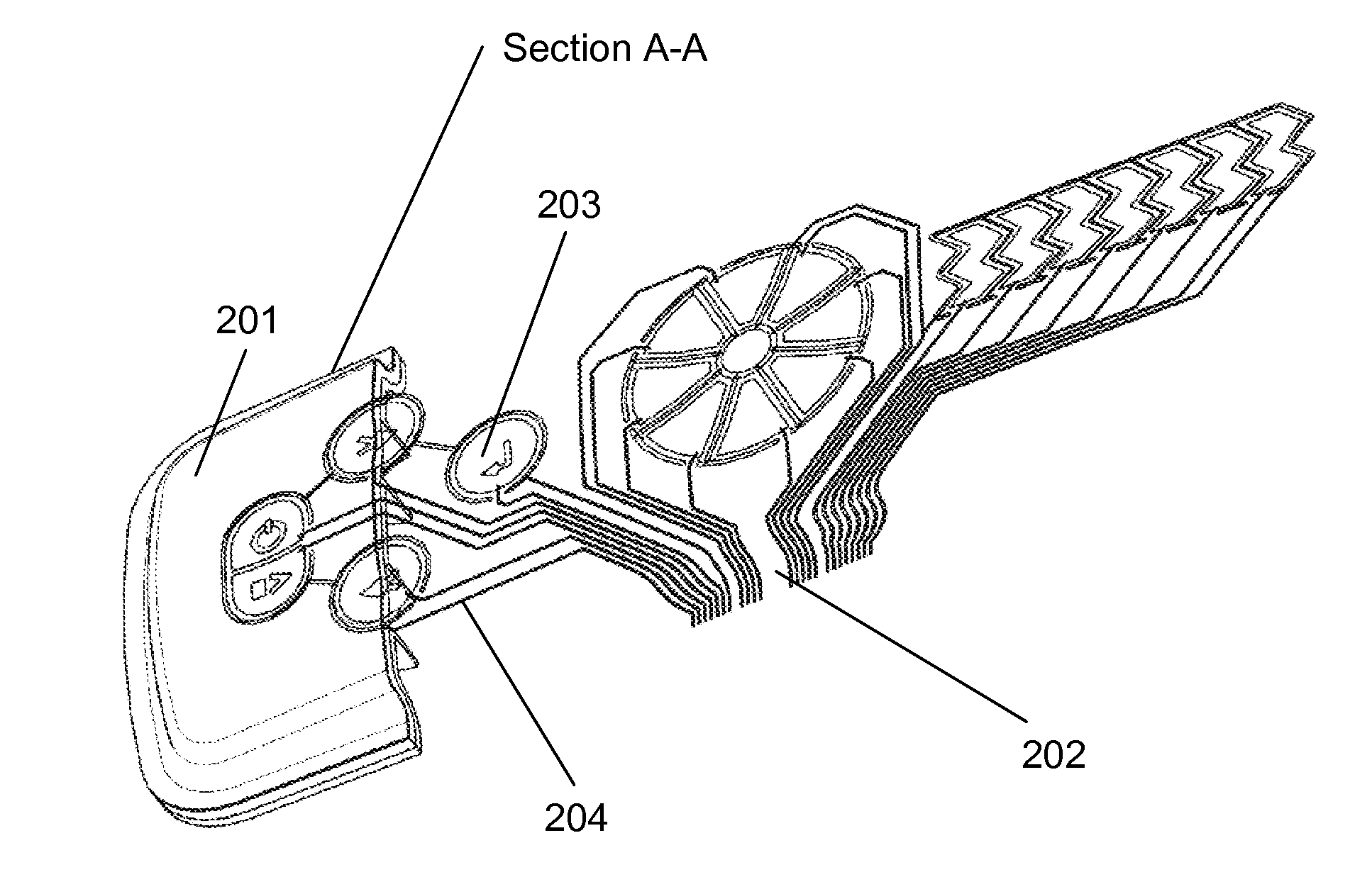
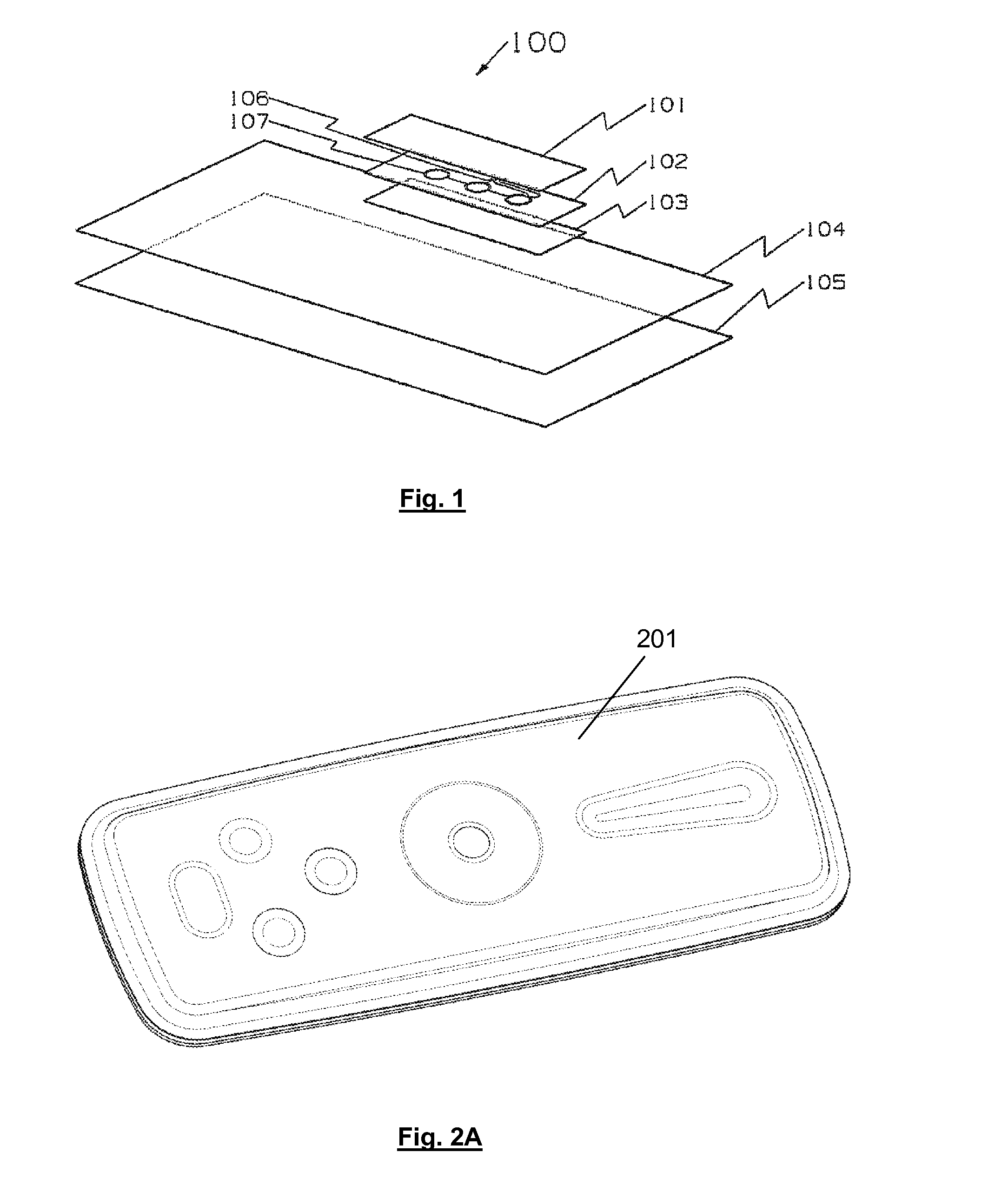
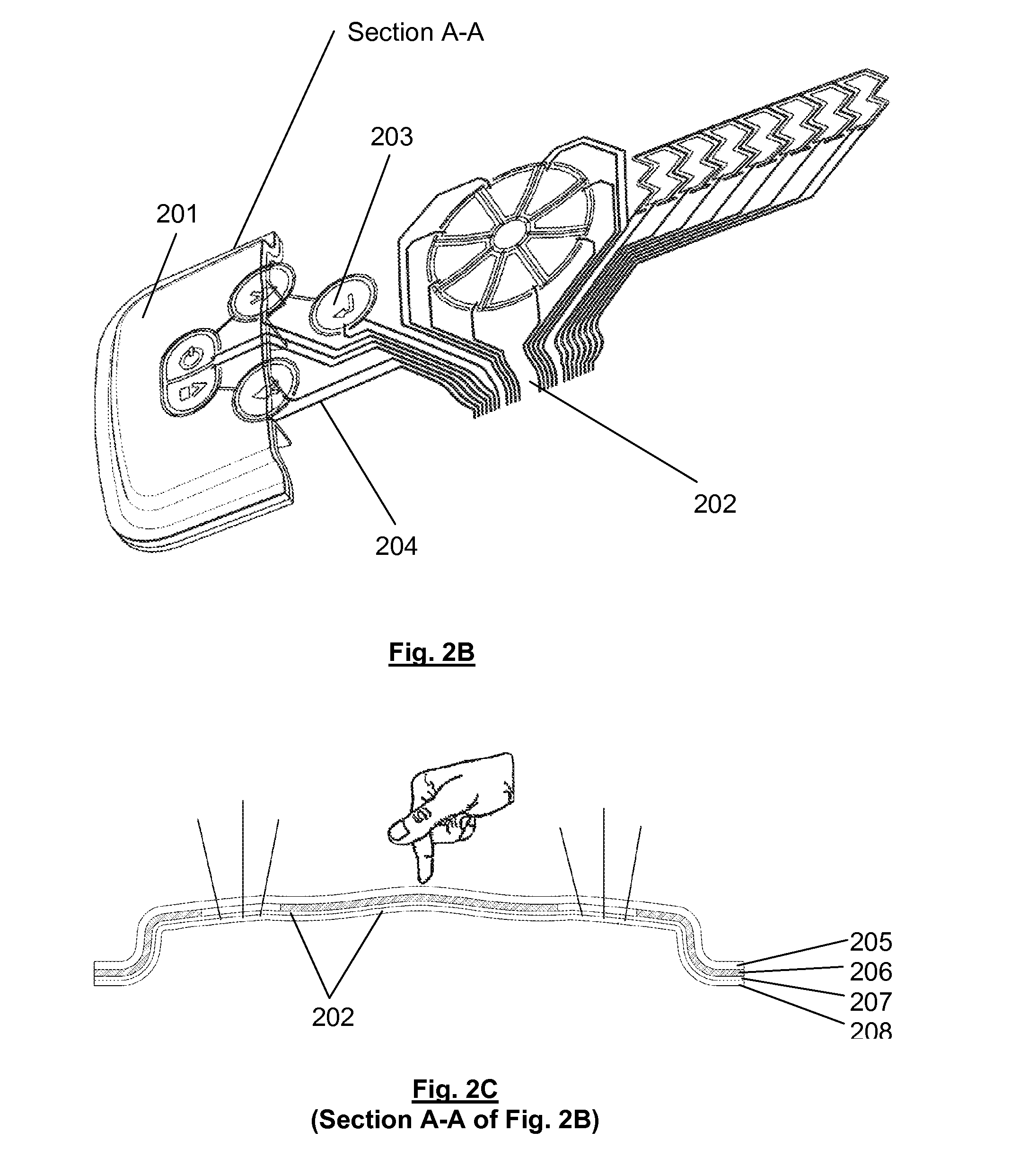
[0047]In an embodiment, a true 3-D moulded article including contours spanning sensing is shown in FIGS. 2A and 2B. A touch panel assembly 200 includes a moulded panel 201 having a functional layer 202, such as an electrical layer made from conductive paste. The functional layer 202 can be a paste configured so as to allow additional flexibility and workability while maintaining characteristics such as conductivity. FIM processes are commonly used for printing decorative designs; the decorative printed surface can be used to apply the functional layer 202, such as by a silkscreen printing process or inkjet printing.

[0048]After the printing process for the functional layer 202 is completed, the functional layer 202 can be formed and worked, such as moulded into the moulded panel 201 to form the touch panel assembly 200. Initial forming or shaping can refer to processes that are used to shape the film permanently include processes such as high pressure forming, thermoforming and the l...


PUM

PropertyMeasurementUnit
widthaaaaaaaaaa
thicknessaaaaaaaaaa
thicknessaaaaaaaaaa

Abstract

A method includes patterning one or more electrical layers on a substrate; shaping the patterned substrate into a 3-dimensional contour, wherein the contour including a significant change in gradient in or adjacent to one or more sensing areas of the electrical layer, and over-molding the shaped substrate. Degradation of a trace in the electrical layer at or adjacent to the one or more sensing areas during shaping and / or over-molding is substantially minimized based on the width of the trace, the thickness or number of layers of the trace, the bending radius of the trace, the material of the trace, and / or a primer over layer on the trace.

Description

FIELD OF THE INVENTION[0001]The present invention relates generally to a method of moulding.CROSS-REFERENCE TO RELATED APPLICATIONS[0002]The present application is a National Stage application of International Application No. PCT / SG2012 / 000379. International Application No. PCT / SG2012 / 000379 was filed in the Intellectual Property Office of Singapore within one-year of and claims priority to both Singapore Application No. 201107618-9 and International Application No. PCT / SG2012 / 000295. Accordingly, this application is a filing under 35 U.S.C. 371 as the National Stage of International Application No. PCT / SG2012 / 000379, filed Oct. 9, 2012, entitled “A METHOD OF MOULDING,” by Chee Seng LEONG, et al., which is a continuation-in-part under 35 U.S.C. 120 of and claims the benefit of International Application No. PCT / SG2012 / 000295, filed Aug. 21, 2012, entitled “A METHOD OF MAKING AN ELECTRONIC APPARATUS INCORPORATING A CONTURED FUNCTIONAL FILM,” by Chee Seng LEONG, et al., and claims fore...

Claims


Application Information

Patent Timeline
Patent Type & Authority Patents(United States)
IPC IPC(8): H03K17/96B29C45/16H01R43/00H05K3/00H05K1/00H05K7/02B29C45/14H05K3/10B29L31/34B29C53/04
CPCB29C45/1671B29C53/04H03K2217/960785H05K3/10B32B2457/00H05K7/02B29L2031/3437H03K2217/960755B29C45/14811H03K17/9622Y10T29/49155Y10T29/49117Y10T29/49156B29C45/14B32B37/18H03K17/96
Inventor LEONG, CHEE SENGCHUA, SZE LAM
Owner FISCHER TECH
Why Eureka
Try Eureka