Semiconductor device

a semiconductor and semiconductor technology, applied in the direction of semiconductor devices, transistors, electrical equipment, etc., can solve the problems of inability to have a high on/off ratio of drain current, inability to have favorable transistor characteristics, and difficulty in high-power applications to be applied to semiconductor devices. achieve the effect of reducing the number of transistors, and increasing the output current per unit area

Inactive Publication Date: 2014-12-16
SEMICON ENERGY LAB CO LTD
View PDF142 Cites 0 Cited by
  • Summary
  • Abstract
  • Description
  • Claims
  • Application Information

AI Technical Summary

Benefits of technology

[0033]The semiconductor device which is one embodiment of the present invention can have favorable transistor characteristics and obtain higher drain current. Moreover, in a semiconductor device which is one embodiment of the present invention, output current per unit area can be increased by connecting a plurality of devices in parallel to each other. Further, in the semiconductor device which is one embodiment of the present invention, by using a metal substrate having high thermal conductivity as a substrate over which a transistor is formed, a heat radiation function can be improved.

Problems solved by technology

The lateral transistor has a thin channel region to be a path of the drain current, and is therefore difficult to be applied to a semiconductor device for high power application.
However, there is a problem in that the vertical transistor using silicon cannot have a high on / off ratio of drain current and thus cannot have favorable transistor characteristics.

Method used


Image

  • Semiconductor device
  • Semiconductor device
  • Semiconductor device

Examples


embodiment 1

(Embodiment 1)

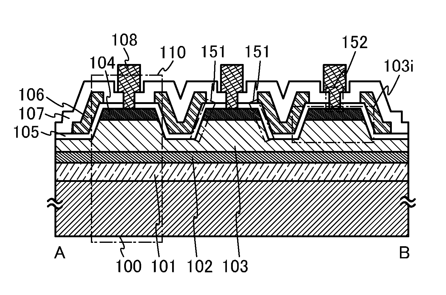
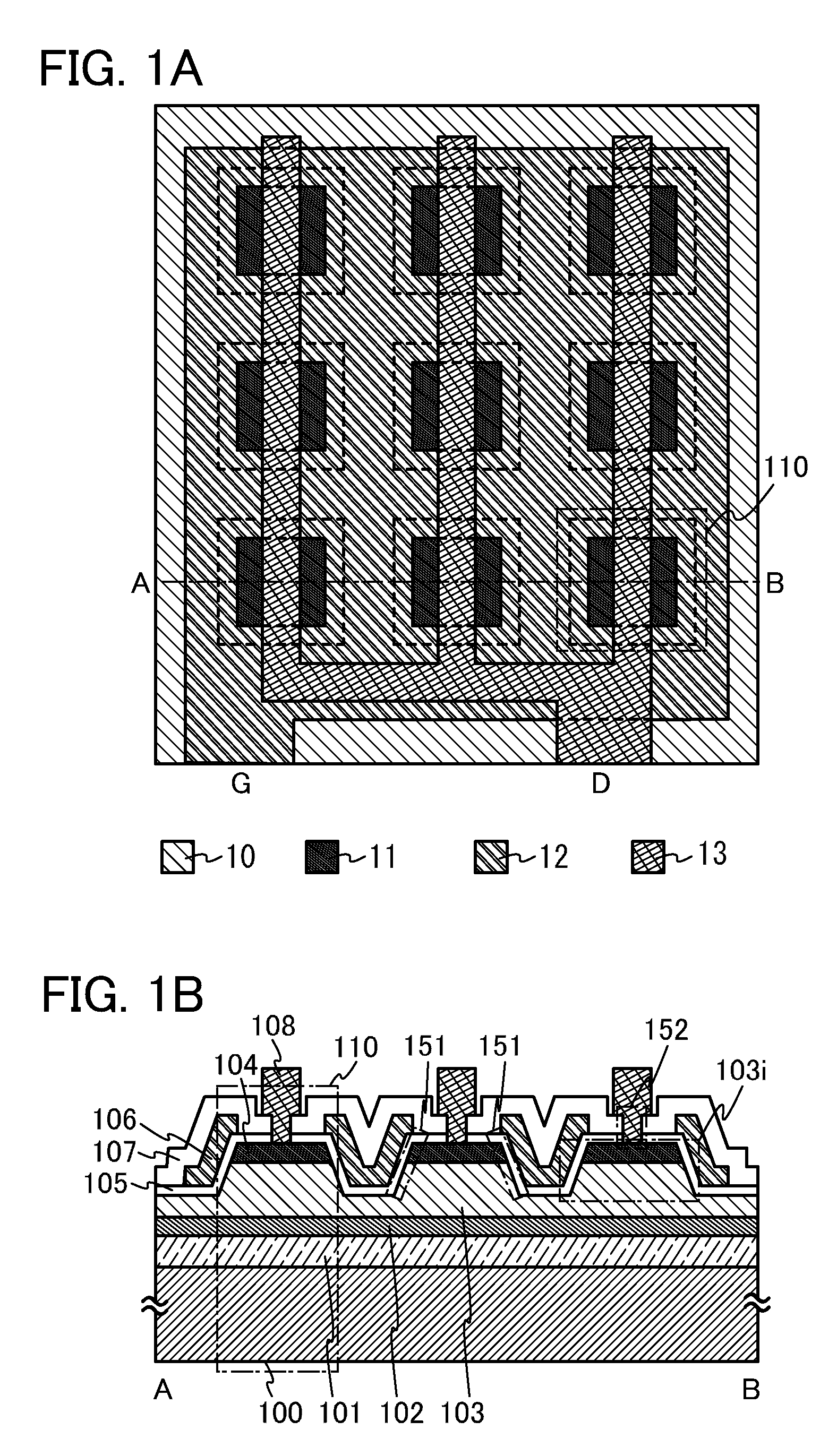
[0055]In this embodiment, a semiconductor device which is one embodiment of the present invention is described with reference to a top view and a cross-sectional view.

[0056]FIG. 1A is a top view of a semiconductor device including a transistor 110, and FIG. 1B is a cross-sectional view taken along line A-B of FIG. 1A.

[0057]FIG. 1A is a top view of the case where a plurality of conductive layers, a plurality of insulating layers, and an oxide semiconductor layer are stacked over a substrate. In FIG. 1A, in particular, a layout diagram of an oxide semiconductor layer 10, a conductive layer 11, a conductive layer 12, and a conductive layer 13 is shown. Note that in FIG. 1A, an insulating layer is not illustrated. Further, in FIG. 1A, a portion where the conductive layers are overlapped with the oxide layer when seen from above is surrounded by a dotted line.

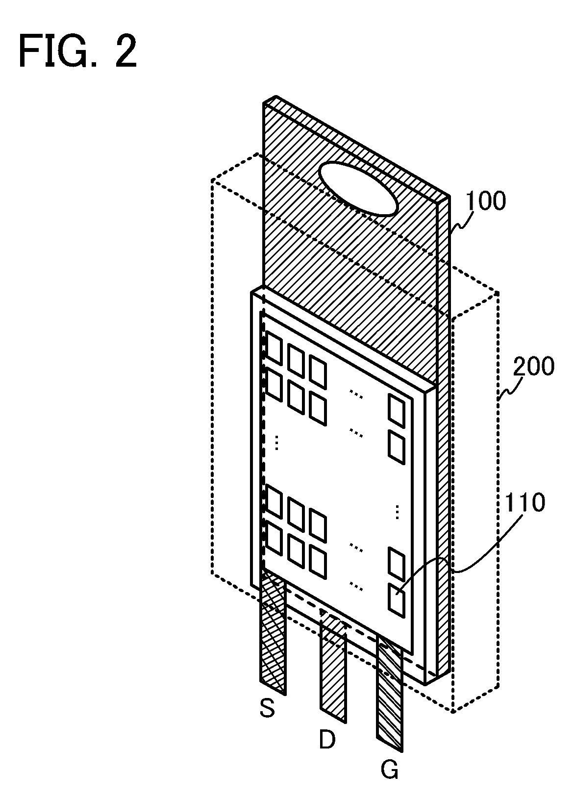
[0058]In FIG. 1A, the plurality of transistors 110 is provided in a dot pattern over the substrate. Though an exampl...

embodiment 2

(Embodiment 2)

[0150]In this embodiment, a semiconductor device having a structure which is different from that of the semiconductor device in Embodiment 1 is described. A transistor having a configuration different from that of the transistor described in Embodiment 1 is described.

[0151]FIG. 12A is a top view of a transistor 210 included in a semiconductor device. FIG. 12B is a cross-sectional view along line A-B of FIG. 12A.

[0152]The top view illustrated in FIG. 12A is a layout view of an oxide semiconductor layer 20, a conductive layer 21, and a conductive layer 22.

[0153]The oxide semiconductor layer 20 in FIG. 12A corresponds to the oxide semiconductor layer 10 in FIG. 1A. The conductive layer 21 in FIG. 12A corresponds to the conductive layer 11 in FIG. 1A. The conductive layer 22 in FIG. 12A corresponds to the conductive layer 12 in FIG. 1A.

[0154]The layout in the top view in FIG. 12A is different from the layout in the top view in FIG. 1A in that a conductive layer which is co...

embodiment 3

(Embodiment 3)

[0162]In this embodiment, one embodiment of the configuration of a power converter circuit such as an inverter, and a converter including the insulated-gate field-effect transistor described in Embodiment 1 and Embodiment 2 is described. In this embodiment, FIGS. 13A and 13B each show an example of the configuration of a DC-DC converter, and FIG. 14 shows an example of the configuration of an inverter.

[0163]A DC-DC converter 501 in FIG. 13A is an example of a step-down DC-DC converter using a chopper circuit. The DC-DC converter 501 includes a capacitor 502, an IGFET 503, a control circuit 504, a diode 505, a coil 506, and a capacitor 507.

[0164]The DC-DC converter 501 in FIG. 13A is operated by a switching operation of the IGFET 503 with the control circuit 504. By the DC-DC converter 501, an input voltage V1 applied to input terminals IN1 and IN2 can be output from output terminals OUT1 and OUT2 to a load 508 as a stepped-down voltage V2 which is stepped down. The sem...


PUM


Abstract

A transistor used for a semiconductor device for high power application needs to have a channel region for obtaining higher drain current. As an example of such a transistor, a vertical (trench type) transistor has been considered; however, the vertical transistor cannot have a high on / off ratio of drain current and thus cannot have favorable transistor characteristics. Over a substrate having conductivity, an oxide semiconductor layer having a surface having a dotted pattern of a plurality of island-shaped regions with a tapered shape in a cross section is sandwiched between a first electrode formed between the substrate and the oxide semiconductor layer and a second electrode formed over the oxide semiconductor layer, and a conductive layer functioning as a gate electrode is formed on the side surface of the island-shaped region in the oxide semiconductor layer with an insulating layer provided therebetween.

Description

BACKGROUND OF THE INVENTION[0001]1. Field of the Invention[0002]The technical field of the present invention relates to a semiconductor device using an oxide semiconductor. In particular, the technical field of the present invention relates to a semiconductor device including a transistor using an oxide semiconductor.[0003]In this specification, a semiconductor device generally means a device which can function by utilizing semiconductor characteristics, and an electrooptic device, a semiconductor circuit, and electronic equipment are all semiconductor devices.[0004]2. Description of the Related Art[0005]Transistors which are used for many liquid crystal display devices and light-emitting display devices typified by flat panel displays have been formed over glass substrates and using a silicon semiconductor such as amorphous silicon or polycrystalline silicon.[0006]Instead of the silicon semiconductor, a technique in which an oxide semiconductor is used for transistors has attracted...

Claims


Application Information

Patent Timeline
Patent Type & Authority Patents(United States)
IPC IPC(8): H01L29/786H01L29/45H01L29/423H01L29/66
CPCH01L29/45H01L29/42384H01L29/78642H01L29/7869
Inventor YAMAZAKI, SHUNPEI
Owner SEMICON ENERGY LAB CO LTD
Why Eureka
Try Eureka