Field-effect transistor, method for producing the same, display element, image display device, and system

a field-effect transistor and display element technology, applied in the field of field-effect transistors, to achieve the effect of favorable transistor characteristics and simple configuration

Active Publication Date: 2021-05-25
RICOH KK
View PDF37 Cites 0 Cited by
  • Summary
  • Abstract
  • Description
  • Claims
  • Application Information

AI Technical Summary

Benefits of technology

[0008]According to the present disclosure, it is possible to provide a field-effect transistor which prevents an oxide semiconductor to be an active layer from being reduced between an interface of the oxide semiconductor with a source electrode and an interface of the oxide semiconductor with a drain electrode, and has a simple configuration and favorable transistor characteristics.

Problems solved by technology

In that case, there is concern that the resultant transistor becomes a normally-on field-effect transistor where even when gate voltage of the transistor is not applied, a large quantity of electric current flows between the source electrode and the drain electrode.

Method used


Image

  • Field-effect transistor, method for producing the same, display element, image display device, and system
  • Field-effect transistor, method for producing the same, display element, image display device, and system
  • Field-effect transistor, method for producing the same, display element, image display device, and system

Examples


example 1

[0287]

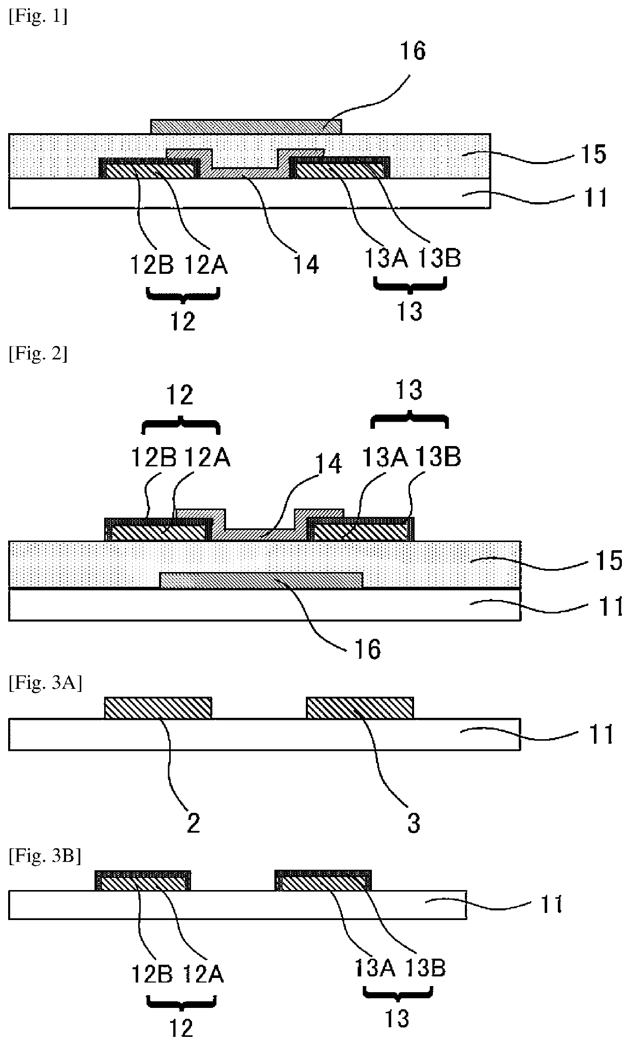
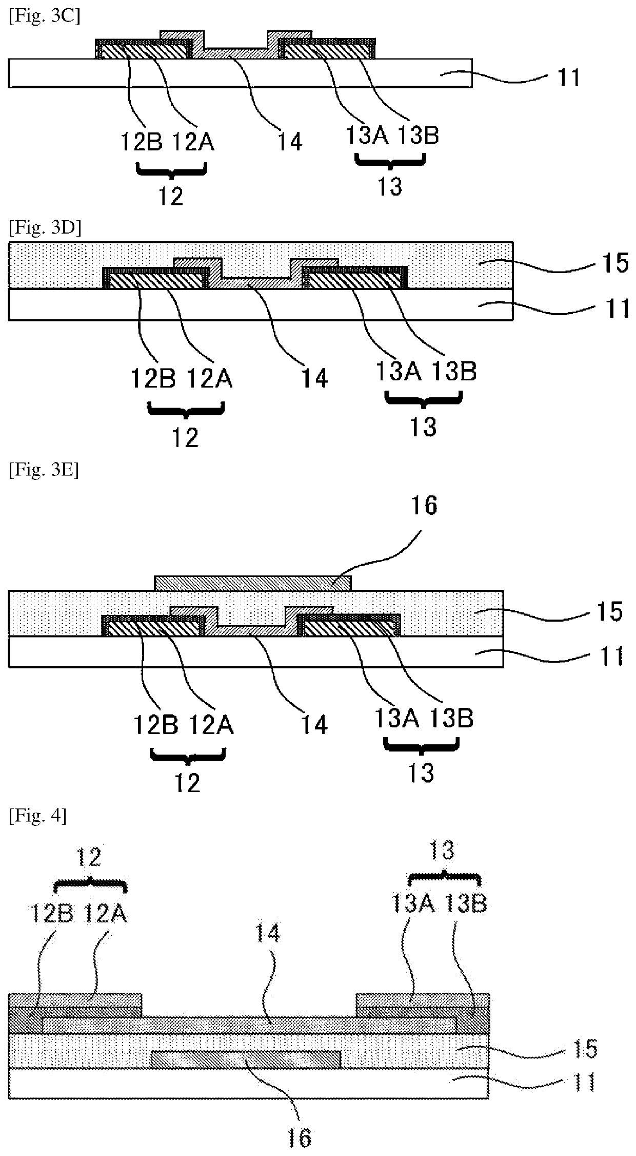
[0288]In Example 1, a top gate / bottom contact field-effect transistor as presented in FIG. 1 was produced. Here, numerical references presented in the following Examples correspond to the numerical references in FIG. 1 and FIGS. 3A to 3E.

[0289]>

[0290]Formation of Source Electrode Precursor and Drain Electrode Precursor

[0291]An Al film to be the second layer was formed on a substrate 11 through a sputtering method so as to have a thickness of 100 nm. Then, a Mo film to be the first layer was formed on the Al film so as to have a thickness of 30 nm.

[0292]Next, resist patterns were formed through photolithography on the formed Al / Mo film and the resultant was subjected to etching to form, on the substrate 11, a metal layer 2 and a metal layer 3 each of which has a predetermined shape.

[0293]—Oxidation Treatment—

[0294]The formed metal layer 2 and the formed metal layer 3 were subjected to heat treatment at 200 degrees Celsius with an oven under the atmosphere to form oxide regions ...

example 2

[0309]

[0310]In Example 2, a top gate / bottom contact field-effect transistor was produced in the same manner as in Example 1 except that the —Formation of source electrode precursor and drain electrode precursor—, the oxidation treatment in the “formation of source electrode and drain electrode”, and the > were changed to the below-described methods.

[0311]The same evaluations as described in Example 1 were performed. Results are presented in Table 1.

[0312]>

[0313]—Formation of Source Electrode Precursor and Drain Electrode Precursor—

[0314]A metal layer 2 and a metal layer 3 were formed in the same manner as in the production steps of the field-effect transistor in Example 1 except that the target used for forming the first layer was changed to each target presented in Table 1.

[0315]—Oxidation Treatment—

[0316]The formed metal layer 2 and metal layer 3 were subjected to plasma treatment in an oxidizing atmosphere under the following conditions to form oxide regions 12B and 13B.

[0317]The...

example 3

[0320]

[0321]In Example 3, a top gate / bottom contact field-effect transistor was produced in the same manner as in Example 1 except that the —Formation of source electrode precursor and drain electrode precursor— and the “formation of active layer” in Example 1 were changed.

[0322]The same evaluations as described in Example 1 were performed. Results are presented in Table 1.

[0323]—Formation of Source Electrode Precursor and Drain Electrode Precursor—

[0324]A metal layer 2 and a metal layer 3 were formed in the same manner as in the production steps of the field-effect transistor in Example 1 except that the target used for forming the first layer was changed to each target presented in Table 1.

[0325]>

[0326]Next, on a region disposed across the source electrode and the drain electrode on the substrate, a film of W-doped MgIn2O4 was formed through a RF magnetron sputtering method so as to have a film thickness of 50 nm. As described above, the surfaces of the source electrode and the dr...


PUM

PropertyMeasurementUnit
electron carrier concentrationaaaaaaaaaa

Abstract

A field-effect transistor including: a gate electrode, which is configured to apply gate voltage; a source electrode and a drain electrode, which are configured to take electric current out; an active layer, which is disposed between the source electrode and the drain electrode and is formed of an oxide semiconductor; and a gate insulating layer, which is disposed between the gate electrode and the active layer, the source electrode and the drain electrode each including a metal region formed of a metal and an oxide region formed of one or more metal oxides, and a part of the oxide region in each of the source electrode and the drain electrode being in contact with the active layer, and rest of the oxide region being in contact with one or more components other than the active layer.

Description

TECHNICAL FIELD[0001]The present disclosure relates to a field-effect transistor, a method for producing the same, a display element, an image display device, and a system.BACKGROUND ART[0002]Flat panel displays (FPDs) such as liquid crystal displays (LCDs), organic EL (electroluminescence) displays (OLEDs), and electronic papers are driven by a driving circuit including a thin film transistor (TFT) in which an amorphous silicon or a poly-crystalline silicon is used as an active layer.[0003]In the development of FPDs, there has been attention to produce a TFT including a field-effect transistor, which includes, on a channel forming area of the active layer, an oxide semiconductor film having high carrier mobility and small unevenness between the elements, and to apply the TFT to electric devices or optical devices.[0004]In a field-effect transistor including an oxide semiconductor serving as an active layer, a stacked metal film of Al and a barrier layer including a transition metal...

Claims


Application Information

Patent Timeline
Patent Type & Authority Patents(United States)
IPC IPC(8): H01L29/786H01L29/45H01L29/66
CPCH01L29/7869H01L29/45H01L29/458H01L29/66969H01L29/78618H01L29/78621H10K59/1213G02F1/13H01L29/517
Inventor KUSAYANAGI, MINEHIDEUEDA, NAOYUKINAKAMURA, YUKIABE, YUKIKOMATSUMOTO, SHINJISONE, YUJISAOTOME, RYOICHIARAE, SADANORI
Owner RICOH KK
Why Eureka
Try Eureka