

Field-effect transistor, method for producing the same, display element, image display device, and system
a field-effect transistor and display element technology, applied in the field of field-effect transistors, to achieve the effect of favorable transistor characteristics and simple configuration
- Summary
- Abstract
- Description
- Claims
- Application Information
AI Technical Summary
Benefits of technology
Problems solved by technology
Method used
Image

Examples
example 1
[0287]
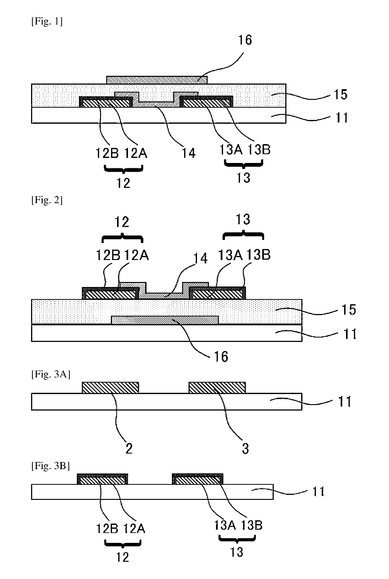
[0288]In Example 1, a top gate / bottom contact field-effect transistor as presented in FIG. 1 was produced. Here, numerical references presented in the following Examples correspond to the numerical references in FIG. 1 and FIGS. 3A to 3E.
[0289]>
[0290]Formation of Source Electrode Precursor and Drain Electrode Precursor
[0291]An Al film to be the second layer was formed on a substrate 11 through a sputtering method so as to have a thickness of 100 nm. Then, a Mo film to be the first layer was formed on the Al film so as to have a thickness of 30 nm.
[0292]Next, resist patterns were formed through photolithography on the formed Al / Mo film and the resultant was subjected to etching to form, on the substrate 11, a metal layer 2 and a metal layer 3 each of which has a predetermined shape.
[0293]—Oxidation Treatment—
[0294]The formed metal layer 2 and the formed metal layer 3 were subjected to heat treatment at 200 degrees Celsius with an oven under the atmosphere to form oxide regions ...
example 2
[0309]
[0310]In Example 2, a top gate / bottom contact field-effect transistor was produced in the same manner as in Example 1 except that the —Formation of source electrode precursor and drain electrode precursor—, the oxidation treatment in the “formation of source electrode and drain electrode”, and the > were changed to the below-described methods.
[0311]The same evaluations as described in Example 1 were performed. Results are presented in Table 1.
[0312]>
[0313]—Formation of Source Electrode Precursor and Drain Electrode Precursor—
[0314]A metal layer 2 and a metal layer 3 were formed in the same manner as in the production steps of the field-effect transistor in Example 1 except that the target used for forming the first layer was changed to each target presented in Table 1.
[0315]—Oxidation Treatment—
[0316]The formed metal layer 2 and metal layer 3 were subjected to plasma treatment in an oxidizing atmosphere under the following conditions to form oxide regions 12B and 13B.
[0317]The...
example 3
[0320]
[0321]In Example 3, a top gate / bottom contact field-effect transistor was produced in the same manner as in Example 1 except that the —Formation of source electrode precursor and drain electrode precursor— and the “formation of active layer” in Example 1 were changed.
[0322]The same evaluations as described in Example 1 were performed. Results are presented in Table 1.
[0323]—Formation of Source Electrode Precursor and Drain Electrode Precursor—
[0324]A metal layer 2 and a metal layer 3 were formed in the same manner as in the production steps of the field-effect transistor in Example 1 except that the target used for forming the first layer was changed to each target presented in Table 1.
[0325]>
[0326]Next, on a region disposed across the source electrode and the drain electrode on the substrate, a film of W-doped MgIn2O4 was formed through a RF magnetron sputtering method so as to have a film thickness of 50 nm. As described above, the surfaces of the source electrode and the dr...
PUM
 Abstract
Description
Claims
Application Information