

Die-stacked memory device with reconfigurable logic
a memory device and logic technology, applied in the field of memory devices, can solve the problems of limiting system flexibility, limiting the broad mass-market appeal of the resulting component, and increasing the cost, complexity, and size of the system
- Summary
- Abstract
- Description
- Claims
- Application Information
AI Technical Summary
Benefits of technology
Problems solved by technology
Method used
Image

Examples
Embodiment Construction
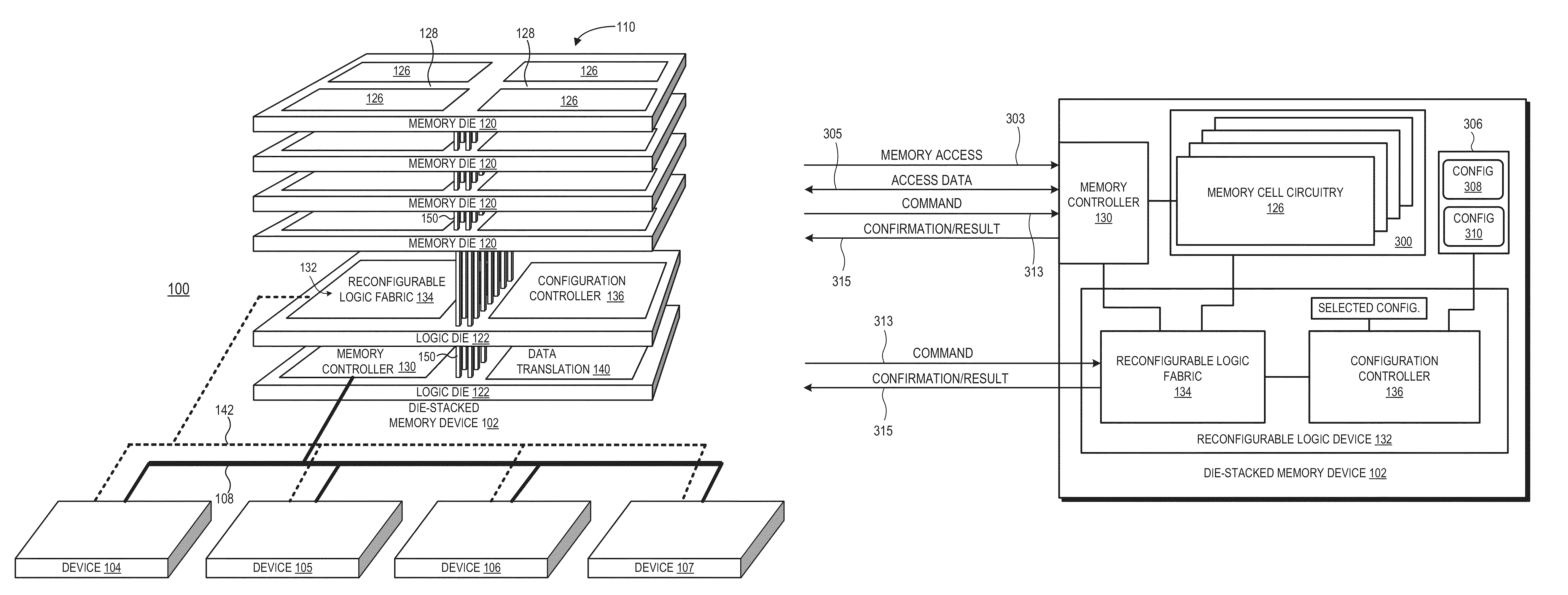
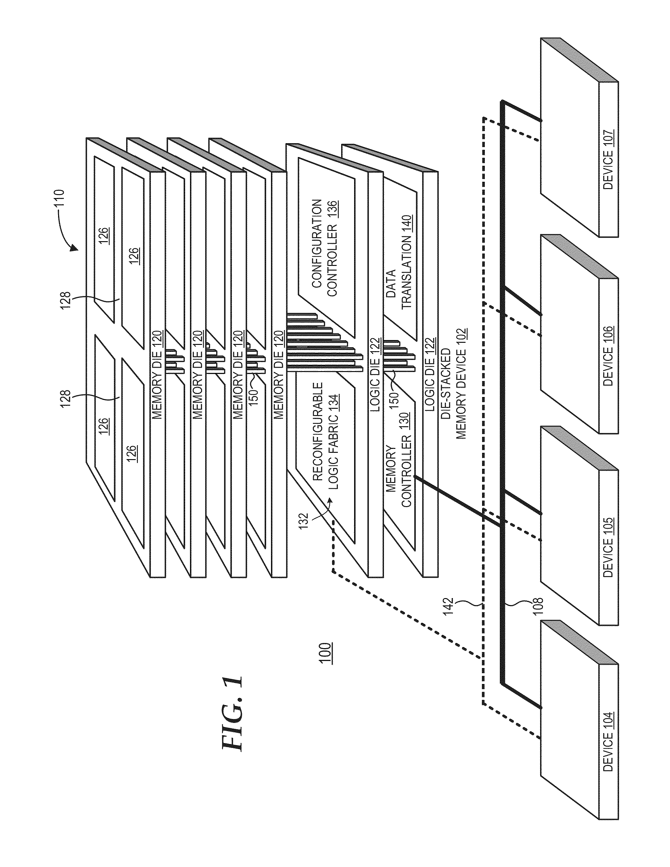
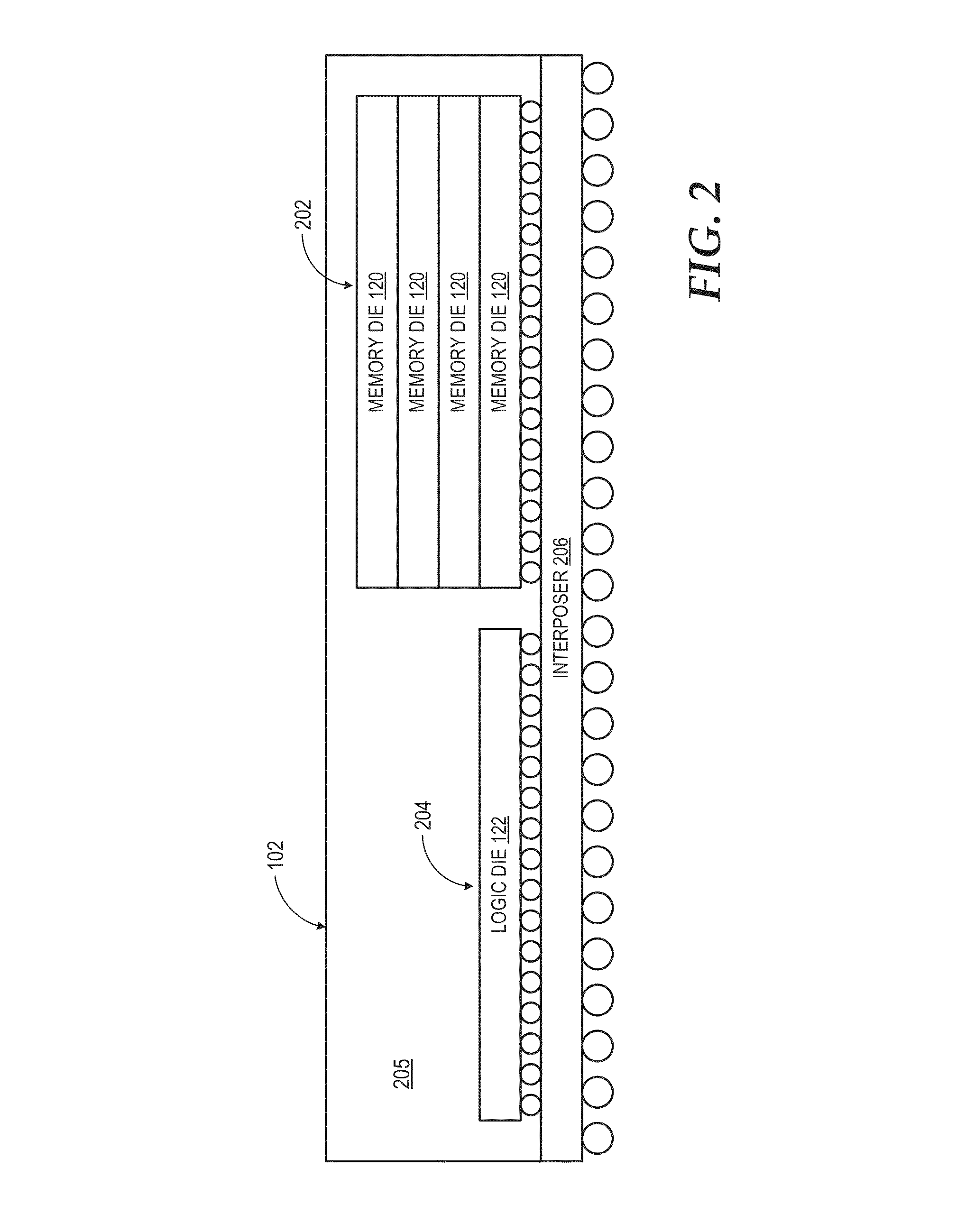
[0017]The following description illustrates example techniques for improved processing efficiency and decreased power consumption in a processing system through the use of a die-stacked memory device incorporating a reconfigurable logic device to provide implementation flexibility in performing various data manipulation operations and other memory operations that use data stored in the die-stacked memory device or that result in data that is to be stored in the die-stacked memory device. The reconfigurable logic device can include, for example, a field-programmable gate array (FPGA), a programmable array logic (PAL) device, a programmable logic array (PLA) device, or a programmable logic device (PLD).
[0018]In some embodiments, one or more configuration files representing corresponding logic configurations for the reconfigurable logic device can be stored in a configuration store at the die-stacked memory device, and a configuration controller can program a reconfigurable logic fabri...
PUM
 Abstract
Description
Claims
Application Information