Semiconductor memory cell, device, and method for manufacturing the same

a memory cell and semiconductor technology, applied in the field of microelectronics, can solve the problems of difficult to reduce the size, difficult to meet the conventional 1t1c structure, and easy loss of stored data, and achieve the effect of high density three-dimensional integration

Active Publication Date: 2015-01-06
INST OF MICROELECTRONICS CHINESE ACAD OF SCI
View PDF17 Cites 4 Cited by
  • Summary
  • Abstract
  • Description
  • Claims
  • Application Information

AI Technical Summary

Benefits of technology

[0021](3) The process for manufacturing the structure according to the present disclosure is completely compa

Problems solved by technology

However, stored data will easily get lost in case of power-off.
With scaling-down of the memory cell, it has become difficult for the conventional 1T1C structure to satisfy requirements such as low leakage current of the transistor and large storage capability of the capacitor.
Meanwhile, for either a trench-type capacitor or a stack-type capacitor, it is difficult to reduce the size thereof while ensuring a capacitance larger than 25 pF.
Though the FBC cell structure has many advantages in terms of pro

Method used


Image

  • Semiconductor memory cell, device, and method for manufacturing the same
  • Semiconductor memory cell, device, and method for manufacturing the same
  • Semiconductor memory cell, device, and method for manufacturing the same

Examples


Embodiment Construction

[0031]The present disclosure will be further explained in detail in connection with specific embodiments and with reference to the drawings, so that objects, technical solutions and beneficial effects thereof will become more apparent.

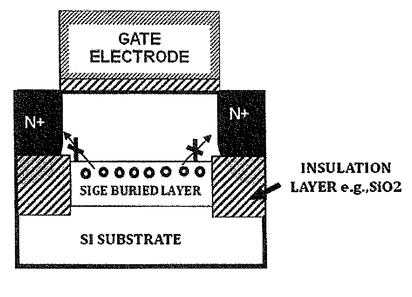
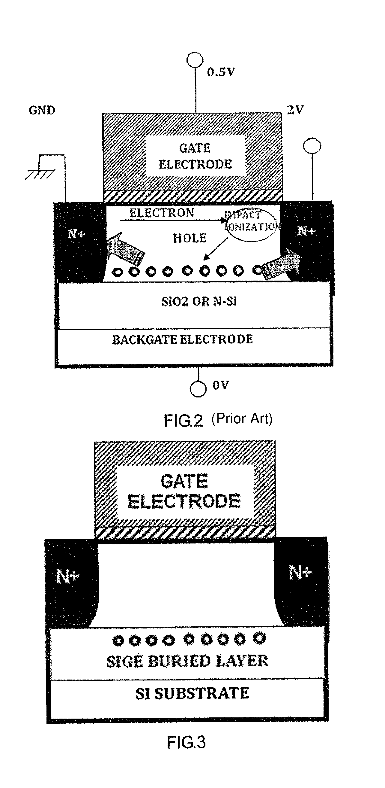
[0032]FIG. 3 is a schematic view showing a semiconductor memory cell according to an embodiment of the present disclosure. As shown in FIG. 3, the semiconductor memory cell comprises: a substrate; a channel region on the substrate; a gate region above the channel region; a source region and a drain region on the substrate and at opposite sides of the channel region; and a buried layer, which is disposed between the substrate and the channel region and comprises a material having a forbidden band narrower than that of a material for the channel region. The substrate may or may not have a back electrode formed thereon.

[0033]According to an embodiment, the channel region may comprise Si or stressed Si, and the buried layer may comprise an IV group materia...


PUM


Abstract

A semiconductor memory cell, a semiconductor memory device, and a method for manufacturing the same are disclosed. The semiconductor memory cell may comprise: a substrate; a channel region on the substrate; a gate region above the channel region; a source region and a drain region on the substrate and at opposite sides of the channel region; and a buried layer, which is disposed between the substrate and the channel region and comprises a material having a forbidden band narrower than that of a material for the channel region material. The buried layer material has a forbidden band narrower than that of the channel region material, so that a hole barrier is formed in the buried layer. Due to the barrier, it is difficult for holes stored in the buried layer to leak out, resulting in an improved information holding duration of the memory cell utilizing the floating-body effect.

Description

CROSS-REFERENCE TO RELATED APPLICATION[0001]This application is National Phase application of, and claims priority to, PCT / CN2011 / 076683, filed on Jun. 30, 2011, entitled “SEMICONDUCTOR MEMORY CELL, DEVICE, AND METHOD FOR MANUFACTURING THE SAME”, which claims priority to the Chinese Patent Application No. 201010541159.6, filed on Nov. 10, 2010, both the PCT Application and Chinese Application are incorporated herein by reference in their entireties.TECHNICAL FIELD[0002]The present disclosure relates to the technical field of microelectronics. In particular, the present disclosure relates to a semiconductor memory cell, a semiconductor memory device, and a method for manufacturing the same.BACKGROUND[0003]Microelectronics products are generally classified into two categories: logic devices and memory devices. As an important type of memory devices, Dynamic Random Access Memories (DRAMs) can support high-speed reading / writing of data. However, stored data will easily get lost in case ...

Claims


Application Information

Patent Timeline
IPC IPC(8): H01L29/06H01L31/00H01L29/78
CPCH01L29/7841Y10S438/933Y10S438/938
Inventor HUO, ZONGLIANGLIU, MING
Owner INST OF MICROELECTRONICS CHINESE ACAD OF SCI
Why Eureka
Try Eureka