This helps you quickly interpret patents by identifying the three key elements:
Problems solved by technology
Method used
Benefits of technology
Benefits of technology
The present patent describes a type of transformer hybrid that has two coils for dual input. These transformer hybrids have small volumes, are resistant to interference, and have a high power capacity. Additionally, they have a high impedance transformation coefficient, which makes them ideal for use in power amplifiers.
Problems solved by technology
However, one of the main problems of the current CMOS process is the low breakdown voltage and the high substrate loss of the silicon, therefore, the approach of power combination through the transformer or hybrid is proposed in order to reduce the area of the transistors as well as increase the output power and efficiency.
And traditional hybrid that implemented by transmission lines or lots of passive components is too large for chip design.
Method used
Image
Click on the blue label to locate the original text in one second.
Reading with bidirectional positioning of images and text.
Examples
first embodiment
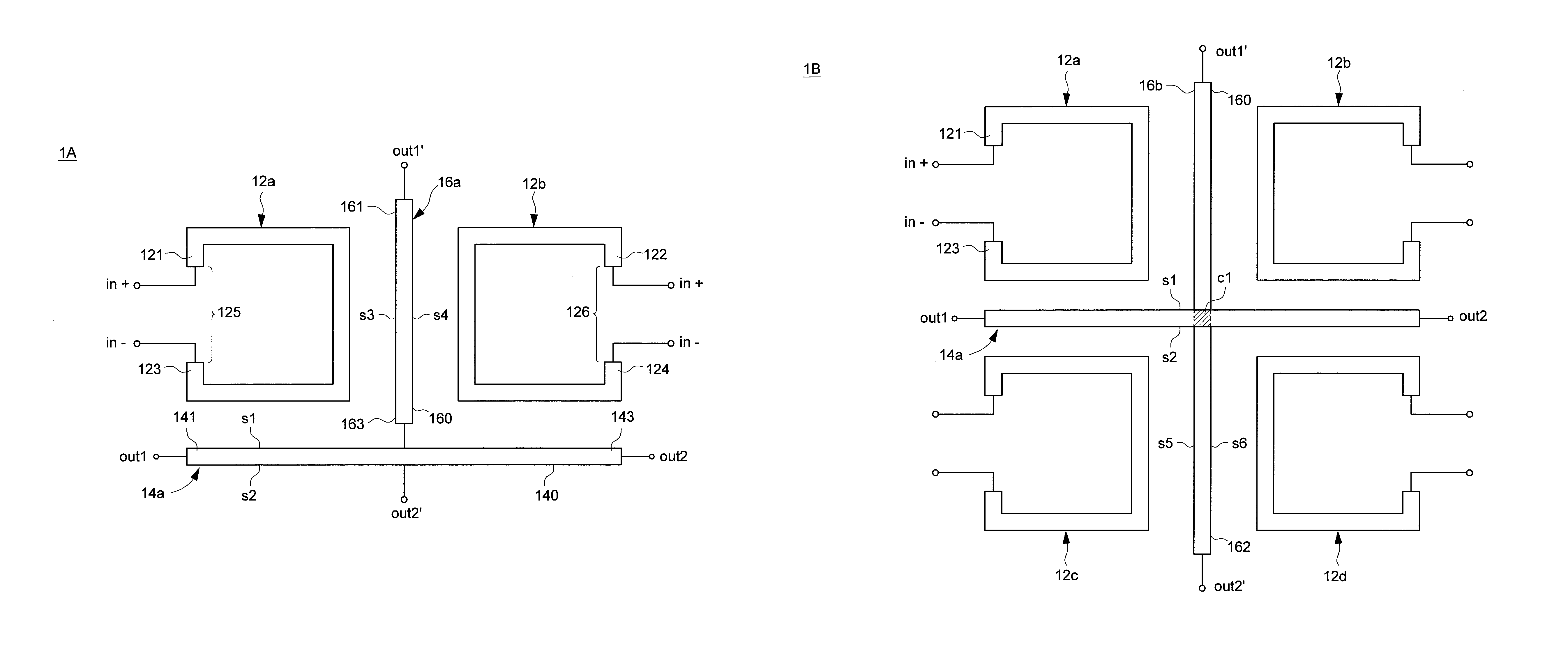
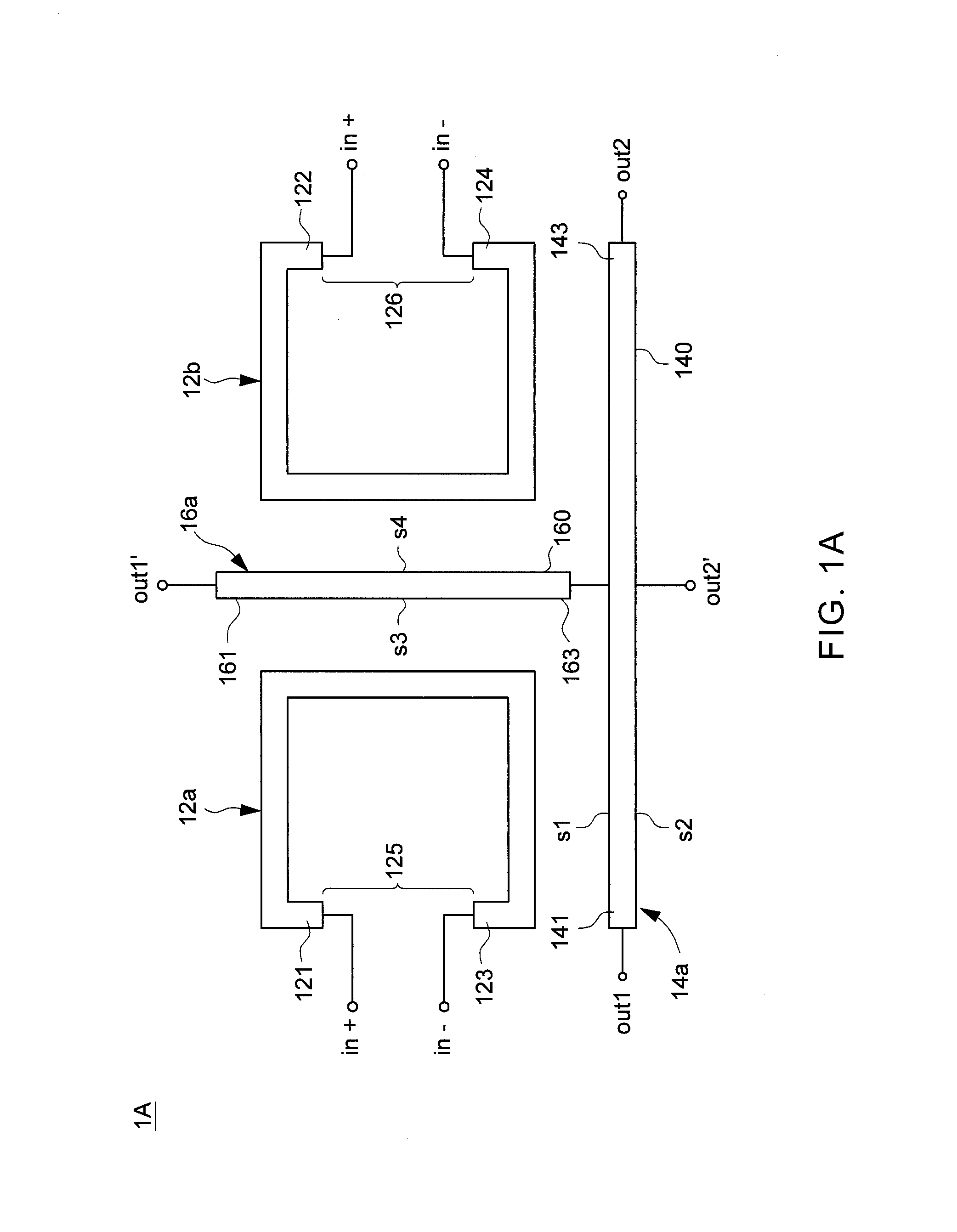
[0020]FIG. 1A depicts a schematic diagram illustrating a transformer hybrid, in accordance with the present disclosure. The transformer hybrid 1A may comprise a substrate (not shown), a first conductor 14a, a second conductor 16a, a first coil 12a, and a second coil 12b. The first conductor 14a, the second conductor 16a, the first coil 12a, and the second coil 12b are formed in the same layer or different layers on the substrate by using the semiconductor process. In other words, the first conductor 14a, the second conductor 16a, the first coil 12a, and the second coil 12b may have different level heights on the substrate. In an embodiment, the substrate may be a ceramic substrate, a silicon substrate or a printed circuit board. In an alternative embodiment, the first conductor 14a, the second conductor 16a, the first coil 12a, and the second coil 12b may be suspended on the substrate by the RFMEMS transformer fabrication process.
[0021]The first coil 12a and the second coil 12b may ...
third embodiment
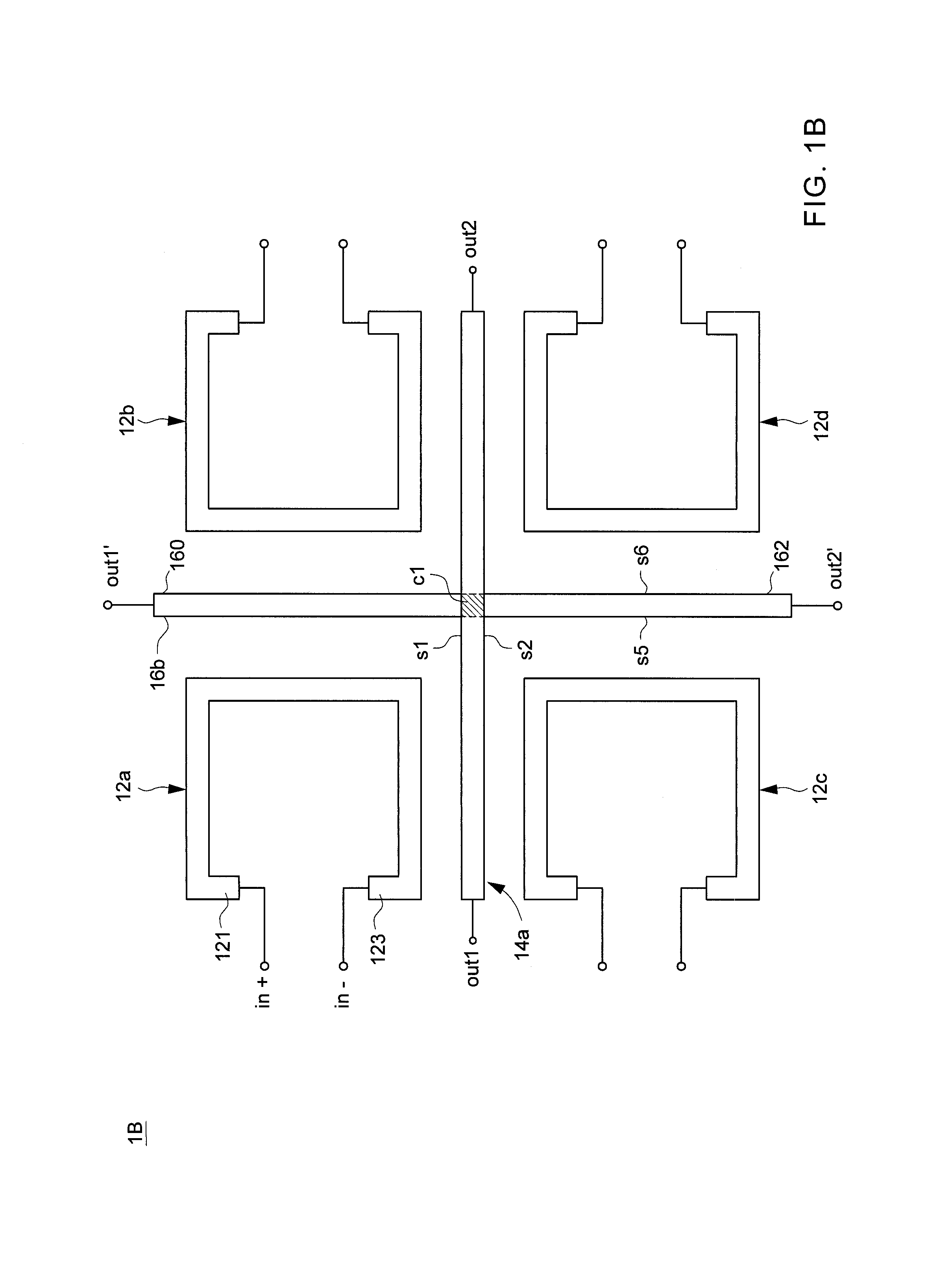
[0035]Alternatively, the transformer hybrid, in accordance with the present disclosure can make a little change. As shown in FIG. 1D, the second conductor 16a can stretch in the horizontal direction from both ends. That is, the second conductor 16a consisted three portions of a vertical part 161, and a first horizontal part 162 and a second horizontal part 163. Those two horizontal parts 162, 163 are parallel located between the coils 12a, 12b and second output terminal 143, first output terminal 143, respectively.
[0036]Alternatively, the transformer hybrid, in accordance with the third embodiment of the present disclosure can make a little more change. As shown in FIG. 1E, the second conductor 16a can stretch further in the vertical direction from both ends. That is, the second conductor 16a consisted five portions of a first vertical parts 161, a second vertical parts 164, a third vertical parts 165, a first horizontal part 162 and a second horizontal part 163. Those two horizonta...
fourth embodiment
[0037]FIG. 2 depicts a schematic diagram illustrating a transformer hybrid, in accordance with the present disclosure. The transformer hybrid 2 comprises a substrate (not shown), a circular conductor 24, a 8-shape conductor 26, a first coil 22a, and a second coil 22b. The circular conductor 24, the 8-shape conductor 26, the first coil 22a, and the second coil 22b are formed in the same layer or different layers on the substrate by using the semiconductor process. In other words, the circular conductor 24, the 8-shape conductor 26, the first coil 22a, and the second coil 22b may have different level heights on the substrate.
[0038]In an embodiment, the circular conductor 24 comprises a first output terminal 241 and a second output terminal 243. The first output terminal 241 and the second output terminal 243 are spaced apart and opposite with each other or face with each other to form a first opening 245. The 8-shape conductor 26 is disposed on the substrate and surrounded with the ci...
PUM
Abstract
A transformerhybrid is disclosed. The transformerhybrid comprises a substrate, a first conductor, a second conductor, a first coil, and a second coil. The first conductor includes a first elongate portion having a first side and a second side. The second conductor includes a second elongate portion having a third side and a fourth side, and the orientation of the second conductor intersects with that of the first conductor. The first coil is located near the first side and the third side. The second coil is located near the first side and the fourth side. When the direction of the loading current in the first coil is the same with that in the second coil, the first conductor has an inductive electromotive force. When the direction of the loading current in the first coil is different from that in the second coil, the second conductor has another inductive electromotive force. When phase difference exists between the loading currents, the two loading currents can be resolved to common mode and differential mode, so the inductive electromotive forces can be produced on the both conductors.
Description
CROSS-REFERENCE TO RELATED APPLICATION(S)[0001]This application claims priority to Taiwan Patent Application No. 102128174, filed on Aug. 6, 2013, the disclosure of which is hereby incorporated by reference in its entirety.BACKGROUND[0002]1. Field of the Disclosure[0003]The present disclosure relates to a transformerhybrid, and more particularly, to a transformer hybrid with multiple input terminals.[0004]2. Description of the Related Art[0005]As the communication technology such as mobile phone, internet and digital TV become more popular and growth rapidly, the need of high quality and low cost CMOS power amplifier is increasing. However, one of the main problems of the current CMOS process is the low breakdown voltage and the high substrate loss of the silicon, therefore, the approach of power combination through the transformer or hybrid is proposed in order to reduce the area of the transistors as well as increase the output power and efficiency.[0006]However, traditional tran...
Claims
Application Information
Patent Timeline
Application Date:The date an application was filed.
Publication Date:The date a patent or application was officially published.
First Publication Date:The earliest publication date of a patent with the same application number.
Issue Date:Publication date of the patent grant document.
PCT Entry Date:The Entry date of PCT National Phase.
Estimated Expiry Date:The statutory expiry date of a patent right according to the Patent Law, and it is the longest term of protection that the patent right can achieve without the termination of the patent right due to other reasons(Term extension factor has been taken into account ).
Invalid Date:Actual expiry date is based on effective date or publication date of legal transaction data of invalid patent.

