Supercharge Your Innovation With Domain-Expert AI Agents!

Semiconductor device having SSOI substrate with relaxed tensile stress

a technology of ssoi substrate and tensile stress, which is applied in the direction of semiconductor devices, basic electric elements, electrical equipment, etc., can solve the problems of 8 to 15% performance degradation of pfet finfet devices

Inactive Publication Date: 2015-02-03
GLOBALFOUNDRIES U S INC
View PDF38 Cites 3 Cited by
  • Summary
  • Abstract
  • Description
  • Claims
  • Application Information

AI Technical Summary

Benefits of technology

This approach improves the performance of p-type finFET devices by relaxing tensile strain and maintaining the performance of n-type finFET devices without degrading complementary devices, resulting in enhanced electron and hole mobility.

Problems solved by technology

When the global intrinsic stresses in an SSOI substrate exceed a predetermined maximum value (e.g., greater than about 1 GPa), however, the performance of PFET finFET devices may be compromised by 8 to 15%.

Method used


Image

  • Semiconductor device having SSOI substrate with relaxed tensile stress
  • Semiconductor device having SSOI substrate with relaxed tensile stress
  • Semiconductor device having SSOI substrate with relaxed tensile stress

Examples


Embodiment Construction

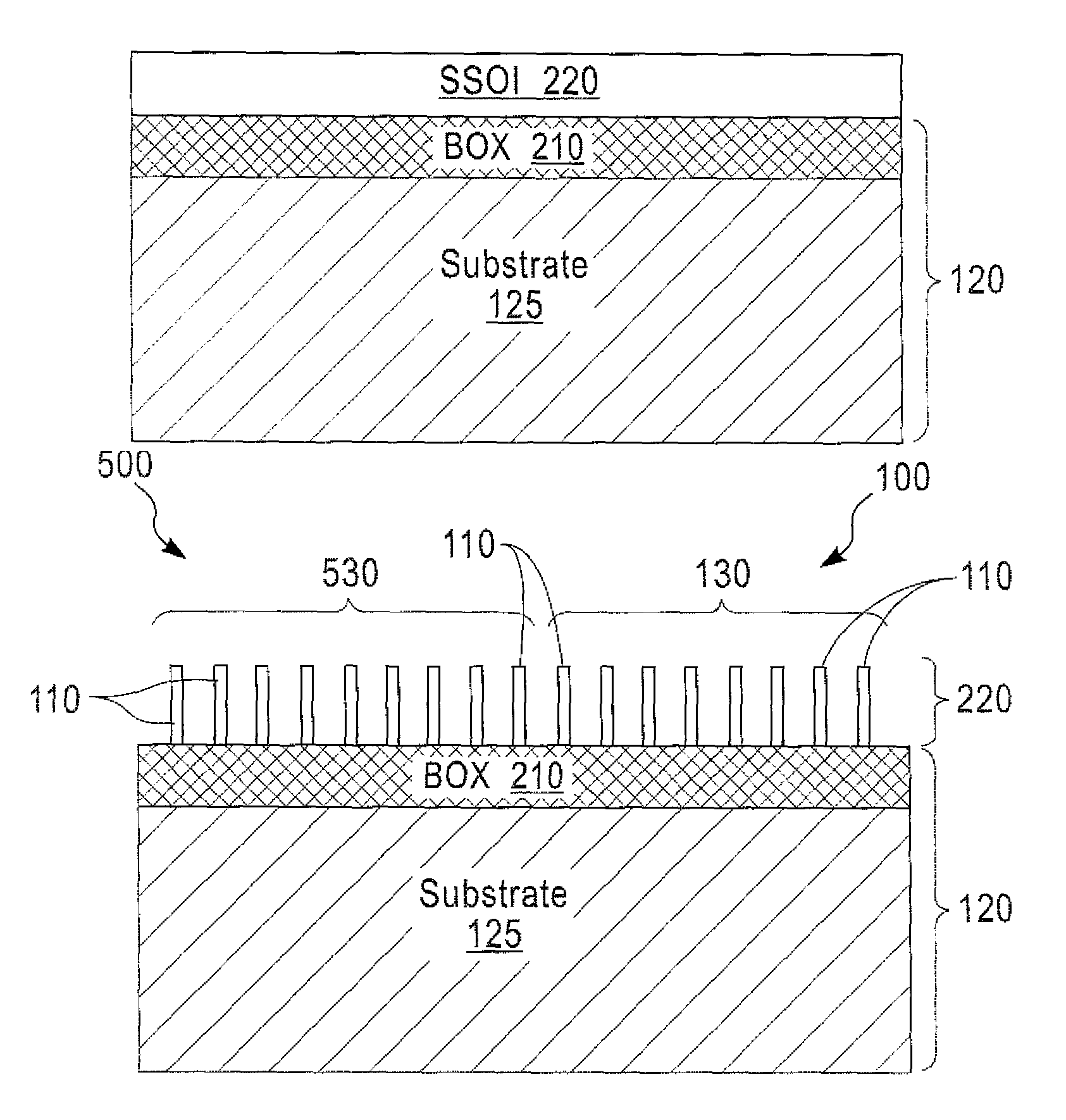
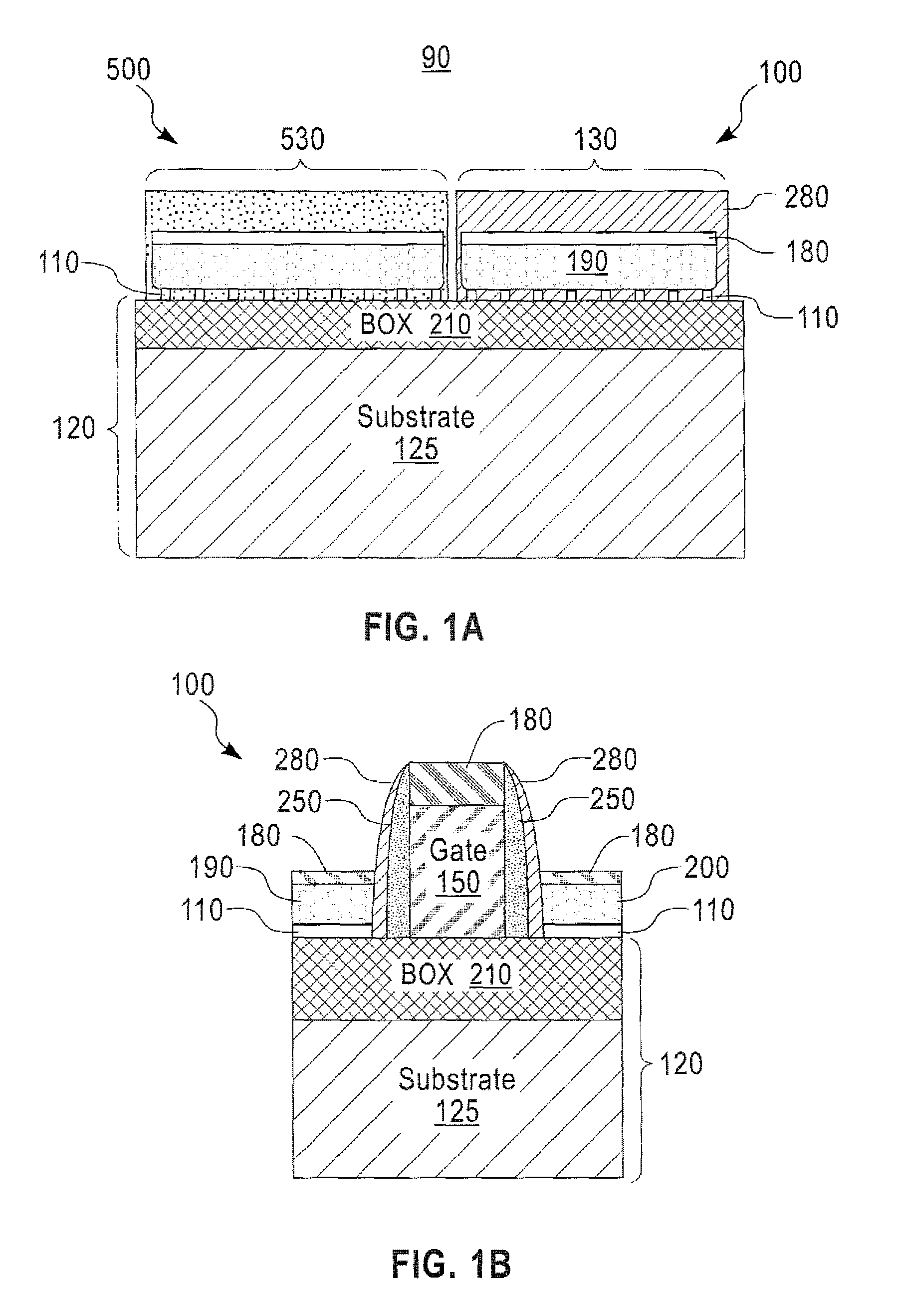
[0024]In exemplary embodiments of the present invention, a semiconductor device is fabricated using a strained silicon-on-insulator (SSOI) layer in which intrinsic tensile stresses are relaxed. Relaxation of the tensile stresses enhances performance of the PFET semiconductor device. Although the semiconductor device is hereinafter referred to as being a PFET, the semiconductor device is not so limited and may comprise an NFET.

[0025]In the fabrication of the PFET, fins are formed from a strained silicon-on-insulator (SSOI) substrate, and gate stack layers and spacers are formed on the fins. Portions of the fins are removed, and the uniaxial tensile strain of the remaining material of the fins is relaxed by subjecting the fins to an elevated temperature (“pre-bake”) for a period of time. Silicon or silicon germanium (SiGe) is epitaxially grown on exposed faces of the fins to merge the source and drain regions. A thin metal layer is deposited on the epitaxially grown silicon or SiGe, a...


PUM

PropertyMeasurementUnit
heightaaaaaaaaaa
heightaaaaaaaaaa
lengthaaaaaaaaaa

Abstract

A method comprises: forming a tensile SSOI layer on a buried oxide layer on a bulk substrate; forming a plurality of fins in the SSOI layer; removing a portion of the fins; annealing remaining portions of the fins to relax a tensile strain of the fins; and merging the remaining portions of the fins.

Description

BACKGROUND[0001]The exemplary embodiments of this invention relate generally to semiconductor devices and, more specifically, to a complementary metal oxide semiconductor device having a strained silicon-on-insulator substrate.[0002]A complementary metal oxide semiconductor device (CMOS) uses complementary and symmetrically-oriented pairs of p-type and n-type metal oxide semiconductor field effect transistors (MOSFETs) arranged on silicon or silicon-on-insulator (SOI) substrates. A MOSFET, which is used for amplifying or switching electronic signals for logic functions, has source and drain regions connected by a channel. The source region is a terminal through which current in the form of majority charge carriers (i.e. electrons or holes) enters the channel, and the drain region is a terminal through which current in the form of majority charge carriers leaves the channel. In a p-type MOSFET (hereinafter “PFET”), the majority charge carriers are holes that flow through the channel,...

Claims


Application Information

Patent Timeline
Patent Type & Authority Patents(United States)
IPC IPC(8): H01L21/20H01L29/78
CPCH01L29/785H01L21/845H01L27/1211H01L29/66795
Inventor BASKER, VEERARAGHAVAN S.KHAKIFIROOZ, ALIKERBER, PRANITAREZNICEK, ALEXANDER
Owner GLOBALFOUNDRIES U S INC
Features
  • R&D
  • Intellectual Property
  • Life Sciences
  • Materials
  • Tech Scout
  • Unparalleled Data Quality
  • Higher Quality Content
  • 60% Fewer Hallucinations
Learn More