Double patterning coloring with color balancing

a patterning and color balancing technology, applied in the field of double patterning coloring with color balancing, can solve the problems of limited light/optics band, limited photolithographic process effectiveness, and difficult to fabricate the geometries or shapes on a single lithographic mask, so as to reduce the overall density of the mask

Active Publication Date: 2015-02-03
CADENCE DESIGN SYST INC
View PDF17 Cites 14 Cited by
  • Summary
  • Abstract
  • Description
  • Claims
  • Application Information

AI Technical Summary

Benefits of technology

[0010]Some embodiments of the invention provide a method for assigning shapes from a layer of an IC design layout to different masks. In order to reduce the density of the masks, the method balances the distribution of features between the masks, re

Problems solved by technology

As more circuit features are packed into an IC design layout (e.g., manufacturing processes at feature sizes of 14 nm and below), the resolution of the photolithographic process makes it extremely difficult to fabricate the geometries or shapes on a single lithography mask.
The difficulty stems from constraining factors in traditional photolithographic processes that limit the effectiveness of current photolithographic processes.
Specifically, the lights/optics are band limited due to physical limitations (e.g., wavelength and aperture) of the photolithographic process.
Therefore, the photolithographic process cannot print beyond a certain minimum width of a feature, minimum spacing b

Method used


Image

  • Double patterning coloring with color balancing
  • Double patterning coloring with color balancing
  • Double patterning coloring with color balancing

Examples


Embodiment Construction

[0032]In the following detailed description of the invention, numerous details, examples, and embodiments of the invention are set forth and described. However, it will be clear and apparent to one skilled in the art that the invention is not limited to the embodiments set forth and that the invention may be practiced without some of the specific details and examples discussed.

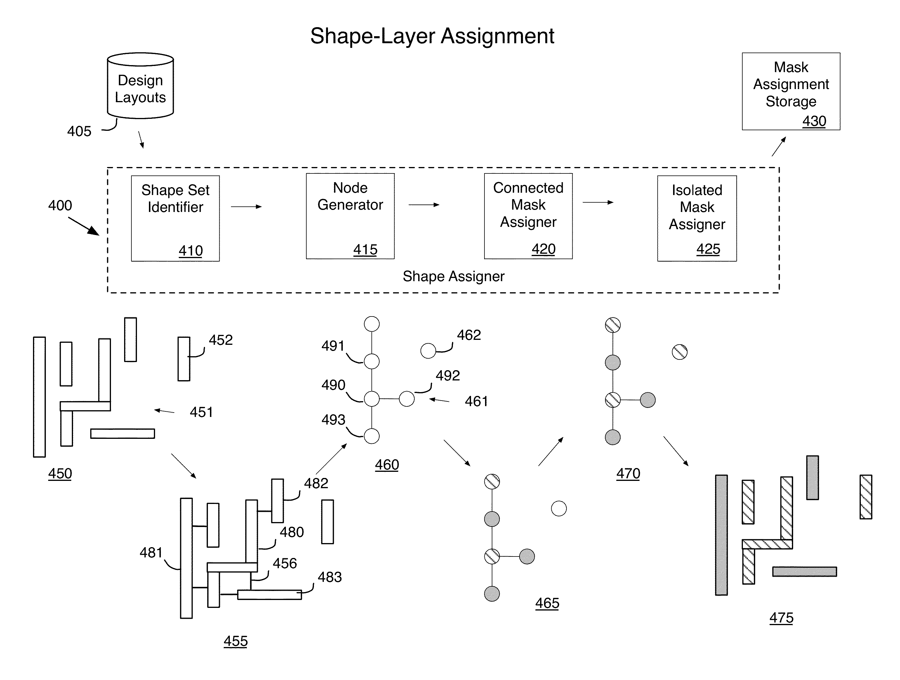
[0033]I. Mask Assignment

[0034]To use DPL technology, the layout designers need to follow a set of design rules or constraints while designing the layout such that the shapes on a single design layer can be successfully fabricated using two different masks. The EDA applications of some embodiments assign two colors (e.g., red and green) to the shapes to identify the two masks with which the shapes will be fabricated. Each shape on a design layer begins with its color unassigned. The EDA application of some embodiments assigns one of the two colors to each shape on the layer. Shapes that have been assigned to th...


PUM


Abstract

Some embodiments of the invention provide a method for balancing the assignment of shapes from a portion of an IC design layout to different masks. The method of some embodiments assigns the shapes to a plurality of masks in a manner that a variation between the numbers of shapes assigned to each mask is within a certain threshold. The method of some embodiments performs a separate analysis for shapes which are outside of a threshold distance from any other shapes.

Description

BACKGROUND[0001]An integrated circuit (“IC”) is a device (e.g., a semiconductor device) or electronic system that includes many electronic components, such as transistors, resistors, diodes, etc. These components are often interconnected to form multiple circuit components, such as gates, cells, memory units, arithmetic units, controllers, decoders, etc. An IC includes multiple layers of wiring that interconnect the IC's electronic and circuit components.[0002]Design engineers design ICs by transforming logical or circuit descriptions of the ICs' components into geometric descriptions, called design layouts. Design layouts typically include (1) circuit modules (i.e., geometric representations of electronic or circuit IC components) with pins and (2) interconnect lines (i.e., geometric representations of wiring) that connect the pins of the circuit modules. In this fashion, design layouts often describe the behavioral, architectural, functional, and structural attributes of the IC. T...

Claims


Application Information

Patent Timeline
IPC IPC(8): G06F17/50
CPCG06F17/5081G06F17/5068G03F1/70G03F7/70283G03F7/70466
Inventor WANG, XIAOJUN
Owner CADENCE DESIGN SYST INC
Why Eureka
Try Eureka