

Programmable logic device and semiconductor device
a logic device and semiconductor technology, applied in logic circuit coupling/interface arrangement, pulse technique, instruments, etc., can solve the problems of increasing circuit area and inhibiting rapid operation of pld, and achieve the effect of increasing operation speed and circuit area
Inactive Publication Date: 2015-02-10
SEMICON ENERGY LAB CO LTD
View PDF148 Cites 15 Cited by
- Summary
- Abstract
- Description
- Claims
- Application Information
AI Technical Summary
Benefits of technology
The present invention relates to a programmable logic device with a novel structure that can operate at high speed, reduce power consumption, and achieve lower power consumption and higher reliability. The invention provides a circuit structure using a pass transistor as a programmable switch element, where the amplitude voltage of a signal applied between programmable logic elements is reduced by the threshold voltage of the pass transistor. To recover the reduced amplitude voltage, a booster circuit such as a pull-up circuit is provided on the output terminal side. The technical effects of this invention are reduced circuit area, increased operation speed, lower power consumption, higher reliability, and suppression of a reduction in amplitude voltage of a signal applied between programmable logic elements.
Problems solved by technology
However, a structure where a pull-up circuit or the like is additionally provided on the output terminal side of a programmable switch element so that a reduced amplitude voltage is recovered to an original amplitude voltage might increase a circuit area and inhibit rapid operation of a PLD.
Method used
View moreImage
Smart ImageViewing Examples

Examples
embodiment 1 (
1. Embodiment 1 (Circuit structure of programmable switch element)
embodiment 2 (
2. Embodiment 2 (Structural example of circuit included in PLD)
embodiment 3 (
3. Embodiment 3 (Circuit operation)
4. Embodiment 4 (Effects of one embodiment of the present invention)
Login to View More PUM
 Abstract
To provide a PLD having a reduced circuit area and an increased operation speed. In the circuit structure, a gate of a transistor provided between an input terminal and an output terminal of a programmable switch element is in an electrically floating state in a period when a signal is input to the programmable switch element. The structure enables the voltage of a gate to be increased by a boosting effect in response to a signal supplied from programmable logic elements, suppressing a reduction in amplitude voltage. This can reduce a circuit area by a region occupied by a booster circuit such as a pull-up circuit and increase operation speed.
Description
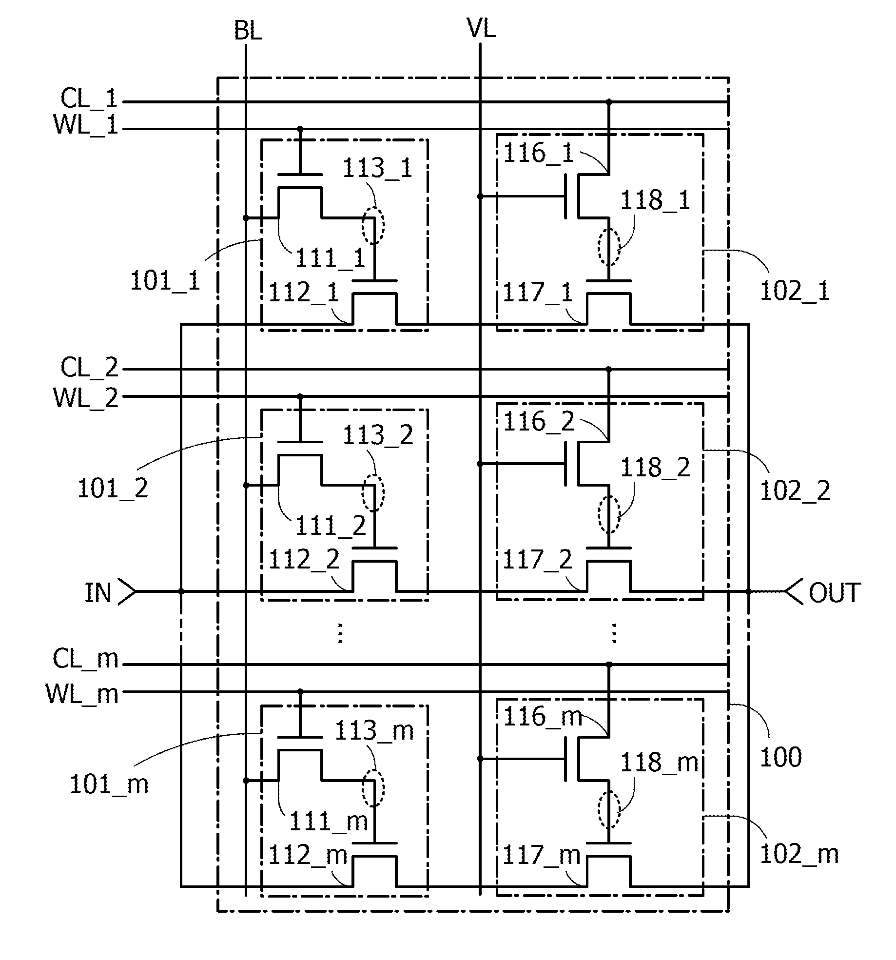
TECHNICAL FIELD[0001]The present invention relates to an object, a method, or a manufacturing method. The present invention relates to a process, a machine, manufacture, or a composition of matter. In particular, the present invention relates to, for example, a semiconductor device, a display device, a light-emitting device, a power storage device, a driving method thereof, or a fabrication method thereof. One embodiment of the present invention particularly relates to a programmable logic device in which the circuit structure can be changed and a semiconductor device or the like including the programmable logic device.BACKGROUND ART[0002]A programmable logic device (PLD) includes a plurality of programmable logic elements and a plurality of programmable switch elements. A circuit structure and a function of the PLD can be varied by changing a function of each programmable logic element or a connection between programmable logic elements that is established with programmable switch ...
Claims
Login to View More Application Information
Patent Timeline
 Patent Type & AuthorityPatents(United States)
IPC IPC(8): H03K19/094H01L25/00H03K19/0175
CPCH03K19/017581H03K19/1776
InventorAOKI, TAKESHIIKEDA, TAKAYUKIKUROKAWA, YOSHIYUKIKOZUMA, MUNEHIRO
OwnerSEMICON ENERGY LAB CO LTD