Semiconductor device

a technology of semiconductor devices and semiconductors, applied in the direction of semiconductor devices, basic electric elements, electrical equipment, etc., can solve the problems of increased production costs, conventional semiconductor devices, etc., and achieve the effect of suppressing the breakdown of semiconductor devices due to local impact ionization

Active Publication Date: 2015-02-24
MITSUBISHI ELECTRIC CORP
View PDF11 Cites 3 Cited by
  • Summary
  • Abstract
  • Description
  • Claims
  • Application Information

AI Technical Summary

Benefits of technology

[0010]The present invention has been made to solve the problems above and an object of the invention is to provide a semiconductor device whose breakdown is effectively prevented without increasing the production cost.
[0012]Regarding the semiconductor device according to the present invention, breakdown of the semiconductor device due to local impact ionization can be suppressed.

Problems solved by technology

Conventional semiconductor devices, however, have the following problems.
Namely, it is necessary for example to additionally implant a predetermined impurity that shortens the lifetime or additionally form a groove for increasing the resistance of a current path, possibly resulting in an increased production cost.

Method used


Image

  • Semiconductor device
  • Semiconductor device
  • Semiconductor device

Examples


first embodiment

[0039]An IGBT will be illustrated here as an example of the semiconductor device according to a first embodiment of the present invention, and a description will be given of a first example of the IGBT.

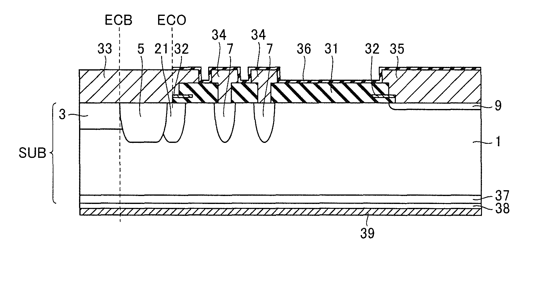
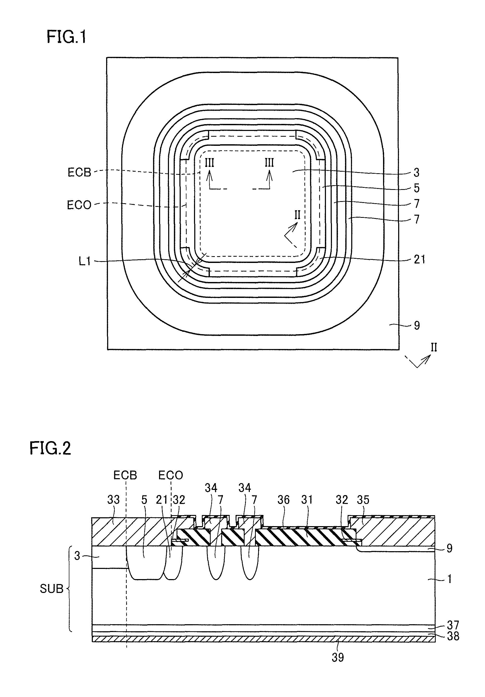
[0040]FIG. 1 is a plan view of the semiconductor device according to the first embodiment of the present invention, FIG. 2 is a cross section along a cross section line II-II shown in FIG. 1, and FIG. 3 is a cross section along a cross section line shown in FIG. 1. In the plan view of FIG. 1, components located on a semiconductor substrate that are depicted in the cross section of FIG. 2 are not shown for the sake of convenience. To be accurate, FIG. 1 illustrates a pattern (prior to heat treatment, corresponding to a mask pattern) for forming each impurity layer to be formed in the semiconductor substrate. The same is applied as well to the plan views referenced hereinafter.

[0041]As shown in FIGS. 1 and 2, an n− layer 1 is formed from one surface (first main surface) of a semiconduct...

second embodiment

[0065]Here, a second example of the IGBT will be described. FIG. 11 is a plan view of a semiconductor device according to a second embodiment of the present invention, and FIG. 12 is a cross section along a cross section line XII-XII shown in FIG. 11. As shown in FIGS. 11 and 12, a p low-concentration layer 21 having a relatively lower impurity concentration is formed in a corner region of p well layer 5. Emitter electrode 33 does not contact p low-concentration layer 21, and an interlayer insulating film 31 is interposed between emitter electrode 33 and p low-concentration layer 21. Since features other than the above-described ones are similar to those shown in FIGS. 1 and 2, the same components are denoted by the same reference characters and the description thereof will not be repeated.

[0066]An operation of the semiconductor device will now be described. The operation of this semiconductor device is basically identical to the operation of the semiconductor device described in co...

third embodiment

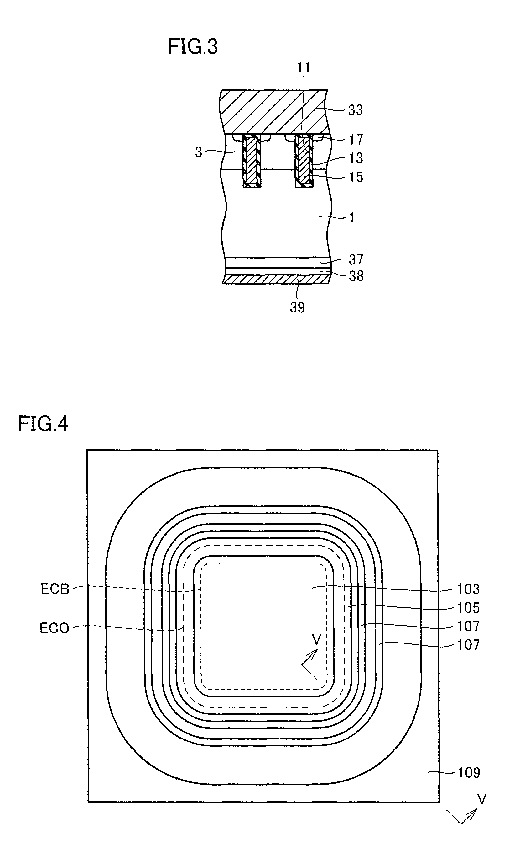
[0070]Here, a third example of the IGBT will be described. FIG. 13 is a plan view of a semiconductor device according to a third embodiment of the present invention, and FIG. 14 is a cross section along a cross section line XIV-XIV shown in FIG. 13. As shown in FIGS. 13 and 14, in a corner region of p well layer 5, p well layer 5 is partially formed in n− layer 1, and a portion (n− layer 22) of n− layer 1 in which p well layer 5 is not formed is located in the shape of an arc along the curve of the corner. Emitter electrode 33 fails to contact this n− layer 22 and also fails to contact the portion of p well layer 5 that is located outside this n− layer 22.

[0071]Furthermore, width W1 of n− layer 22 (the length in the direction substantially orthogonal to the direction of the tangent of the curve of the corner) is designed so that width W1 is larger than twice the width of lateral diffusion of p well layer 5 so as to prevent the portion of p well layer 5 that is located inside n− laye...


PUM


Abstract

In one surface of a semiconductor substrate, an n− layer, a p base layer, a p well layer, another p well layer, a channel stopper layer, an emitter electrode, a guard ring electrode, and a channel stopper electrode for example are formed. In the other surface of the semiconductor substrate, an n+ buffer layer, a p+ collector layer, and a collector electrode are formed. In a curved corner of the p well layer, a p low-concentration layer having a lower impurity concentration than the impurity concentration of the p well layer is formed from the surface to a predetermined depth.

Description

BACKGROUND OF THE INVENTION[0001]1. Field of the Invention[0002]The present invention relates to a semiconductor device and particularly to a semiconductor device for power applications.[0003]2. Description of the Background Art[0004]In general, a high-breakdown-voltage power device is required to block current and keep a high voltage when turned OFF and conduct current with a lowest possible loss when turned ON (ON operation), and further desired to switch between ON and OFF with a lowest possible switching loss.[0005]When the high-breakdown-voltage power device switches from ON to OFF, it is indispensable for this power device to block current without leading to breakdown. The IGBT (Insulated Gate Bipolar Transistor) which is a typical high-breakdown-voltage power device has properties including a reverse biased safe operating area (RBSOA) representing a current-voltage area in which current can be blocked in safety in terms of the fact that the high-breakdown-voltage power device...

Claims


Application Information

Patent Timeline
Patent Type & Authority Patents(United States)
IPC IPC(8): H01L29/739
CPCH01L29/0619H01L29/0696H01L29/404H01L29/7395H01L29/861
Inventor TAKAHASHI, TETSUO
Owner MITSUBISHI ELECTRIC CORP
Why Eureka
Try Eureka