Ultraviolet light emitting diode structures and methods of manufacturing the same

a technology of ultraviolet light and diodes, which is applied in the direction of lasers, semiconductor lasers, solid-state devices, etc., can solve the problems of reducing the efficiency droop of leds under high current injection, and achieve the effects of reducing efficiency droop, improving overall external quantum efficiency, and improving overlap of electron and hole wave functions

Active Publication Date: 2015-03-24
TRUSTEES OF BOSTON UNIV
View PDF41 Cites 6 Cited by
  • Summary
  • Abstract
  • Description
  • Claims
  • Application Information

AI Technical Summary

Benefits of technology

[0012]In this invention, new epitaxial designs are presented for UV and visible light LEDs which reduce efficiency droop and which also increase overall external quantum efficiency (EQE). This is accomplished by designing the active region such that the potential energy height and / or the thickness of the inner barrier layers (“tunable inner barrier” or TIB layers) is optimized to improve overlap of the electron and hole wave-functions, with consequent reduction in the QCSE. Simultaneously, the epitaxial design of the invention allows for high carrier concentration in the wells without using thick individual well layers, and thus reduces the efficiency droop of LEDs under high current injection.
[0015]Yet another aspect of this invention is a method of designing the active region (e.g., multiple quantum wells (MQW)) of a semiconductor light emitting device, such as an LED. The layers of the active region are designed to achieve improved electron-hole wave-function overlap and carrier transport. The resulting epitaxial design can be used to produce the semiconductor structure or semiconductor device described above. The method involves tuning the TIB layer within certain ranges of thickness and / or potential energy level with respect to the outer barrier layers of the active region. In one embodiment for designing a UV-LED, the design starts from a desired LED emission wavelength, chooses the appropriate AlN mole fraction in the well layers and outer barrier layers for that emission wavelength, and selects a tuning mechanism for the TIB layer (i.e., thickness, potential energy, or both). The resulting epitaxial design defines the MQW structure and optimizes device performance, achieving reduced efficiency droop at high current operation.
[0019]In an example, the present invention provides a method of fabricating a light emitting diode device for emission of electromagnetic radiation in an ultraviolet wavelength range. The method includes providing a semiconductor substrate comprising a surface region. The method includes forming a semiconductor structure overlying the surface region. The semiconductor structure is an active region of the light emitting device. The structure comprises two or more well layers, one or more separation layers configured between the well layers. The one or more separation regions is configured to have a first mode to act as one or more barrier regions separating a plurality of carriers in a quantum confined mode in each of the quantum wells being provided on each side of the one or more separation layers and a second mode to cause spreading of the plurality of carriers across each of the quantum wells to increase an overlap integral of all of the plurality of carriers from a first value to a second value, which is greater than the first value. The first value is associated with the first mode and the second value is associated with the second mode.

Problems solved by technology

Simultaneously, the epitaxial design of the invention allows for high carrier concentration in the wells without using thick individual well layers, and thus reduces the efficiency droop of LEDs under high current injection.

Method used


Image

  • Ultraviolet light emitting diode structures and methods of manufacturing the same
  • Ultraviolet light emitting diode structures and methods of manufacturing the same
  • Ultraviolet light emitting diode structures and methods of manufacturing the same

Examples


example 1

Effect of Tunable Barrier Layer Thickness on EQE and Output Power

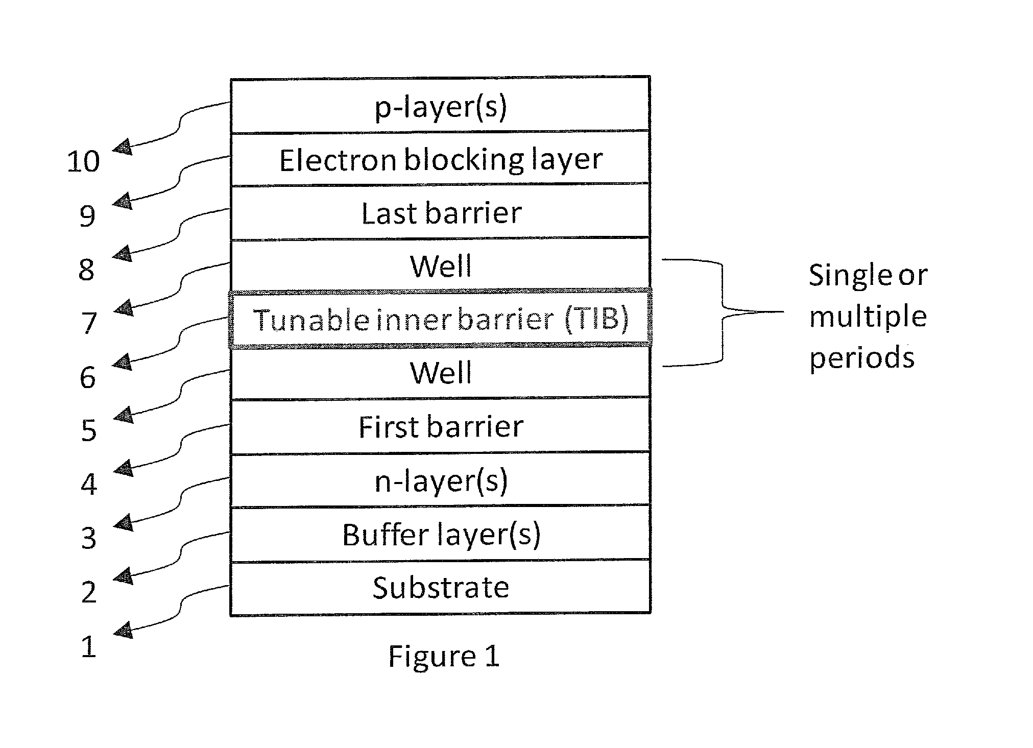
[0072]In this example, results are presented for a series of 280 nm band deep UV LEDs fabricated using identical epitaxial design except for the thicknesses of the TIB layer, which was varied. The epitaxial design of these LEDs is schematically shown in FIG. 4. The AlN mole fraction of the MQW well and barrier layers were within the ranges specified in Tables 3 and 4.

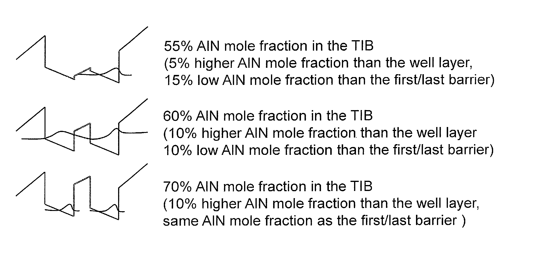
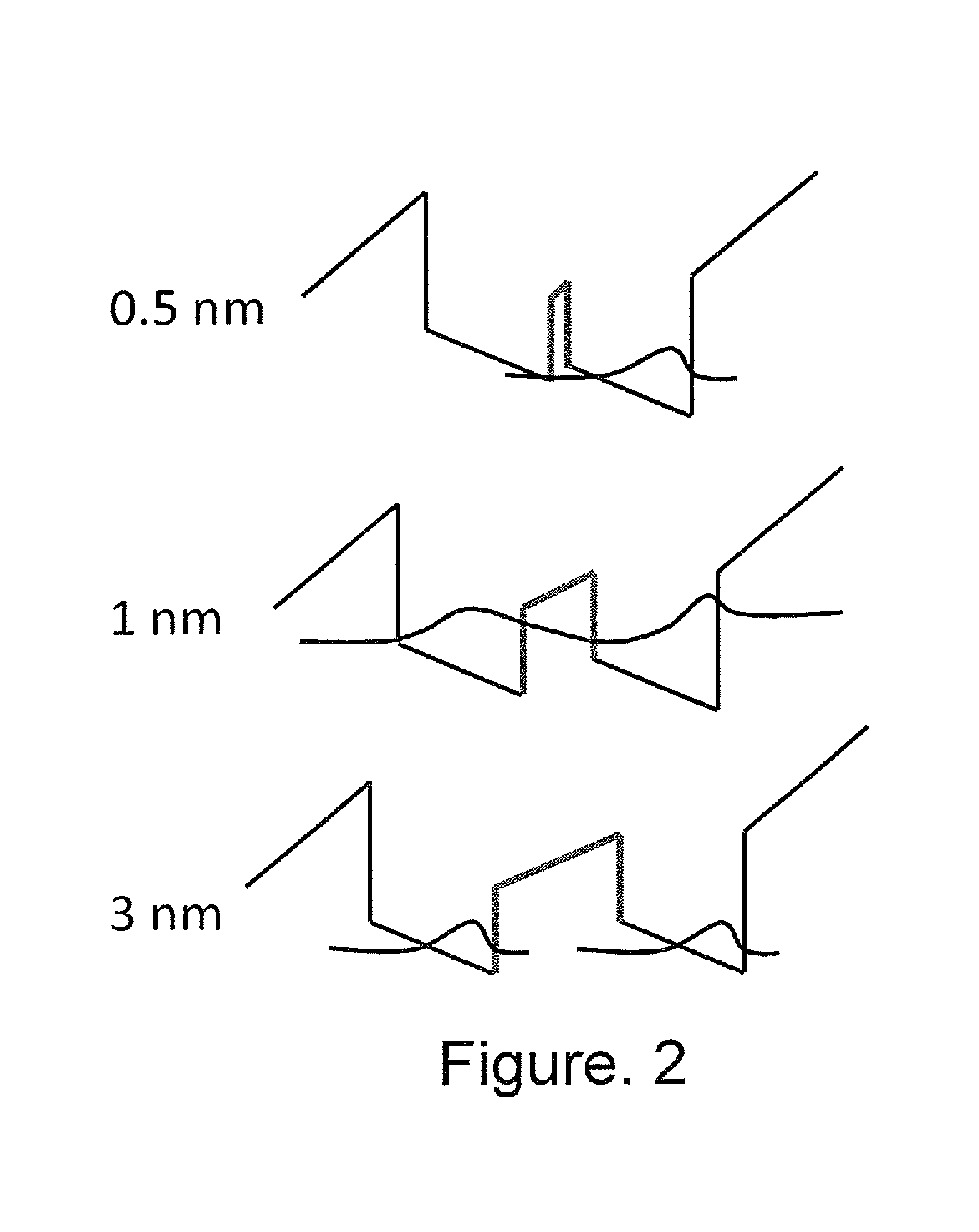
[0073]The TIB layer fabricated with Al0.8Ga0.2N was inserted between two well layers, each having the same AlN mole fraction and fabricated with Al0.65Ga0.35N. The TIB layer had the same AlN mole fraction as the first / last barrier layers and, therefore, only the thickness of the TIB was varied. This allowed investigation of the optimal thickness to reduce efficiency droop of the UV-LED.

[0074]Four UV-LEDs were made with the epitaxial structure shown in FIG. 4, but with different thicknesses of the TIB layer. The thicknesses were 0.5 nm (sample V2769-D), 1 n...

example 2

Effect of Tunable Barrier Layer Thickness on Emission Spectrum

[0079]The emission spectra of the 4 LEDs with different TIB layer thickness described in Example 1 was investigated. The results are shown in FIG. 7. As the TIB layer thickness was reduced from 3 nm to 1 nm, a slight red-shift in the emission spectra was observed. However, when the TIB thickness was reduced to 0.5 nm, wave-function delocalization took place, and strong QCSE further red shifted the emission spectrum by 5 nm.

example 3

Effect of Tunable Inner Barrier Layer Optimization on High Current Density Operation

[0080]Comparing UV-LEDs with multiple quantum wells separated by TIB barrier layers (V2769-C, devices B2, E1 and B1) to enhance carrier transport and wave-function overlap to a single quantum well UV-LED (V2706, devices B, C, and D), it was discovered that the UV-LED with a tuned inner barrier layer could be driven at much higher current density than a single quantum well LED without power output saturation (FIG. 8). This is indicative of the ability of the UV-LED with a tuned inner barrier layer to spread the injected carriers across the multiple quantum wells (two wells in this case). Therefore, at the same drive current the carrier density in the well was lower than for single quantum well UV-LEDs.


PUM


Abstract

Semiconductor structures involving multiple quantum wells provide increased efficiency of UV and visible light emitting diodes (LEDs) and other emitter devices, particularly at high driving current. LEDs made with the new designs have reduced efficiency droop under high current injection and increased overall external quantum efficiency. The active region of the devices includes separation layers configured between the well layers, the one or more separation regions being configured to have a first mode to act as one or more barrier regions separating a plurality of carriers in a quantum confined mode in each of the quantum wells being provided on each side of the one or more separation layers and a second mode to cause spreading of the plurality of carriers across each of the quantum wells to increase an overlap integral of all of the plurality of carriers. The devices and methods of the invention provide improved efficiency for solid state lighting, including high efficiency ultraviolet LEDs.

Description

CROSS REFERENCE TO RELATED APPLICATIONS[0001]This application claims benefit of the priority of U.S. Provisional Patent Application No. 61 / 583,848 filed Jan. 6, 2012 entitled ULTRAVIOLET LIGHT EMITTING DIODES STRUCTURE AND METHOD OF MANUFACTURING THE SAME.[0002]This application claims the benefit under 35 U.S.C. §120 of U.S. application Ser. No. 13 / 734,333, filed Jan. 4, 2013, the entire disclosure of which is incorporated herein by reference.STATEMENT REGARDING FEDERALLY SPONSORED RESEARCH OR DEVELOPMENT[0003]This invention was made with Government Support under Contract No. W911NF-06-2-0040 awarded by the Army Research Office. The Government has certain rights in the invention.BACKGROUND OF THE INVENTION[0004]LEDs based on InAlGaN multiple quantum wells (MQWs) generally suffer from two problems. The first is the so called “Quantum Confined Stark Effect” (QCSE), which is due to internal electric fields caused by spontaneous and piezoelectric polarization. Specifically, this interna...

Claims


Application Information

Patent Timeline
Patent Type & Authority Patents(United States)
IPC IPC(8): H01L33/06H01L33/00H01S5/343
CPCH01L33/0025H01L33/06H01L33/0062H01S5/343H01L33/32H01S5/34333H01S5/34346B82Y20/00H01L33/04G06F30/00H01L33/145
Inventor LIAO, YITAOMOUSTAKAS, THEODORE D.
Owner TRUSTEES OF BOSTON UNIV
Why Eureka
Try Eureka