

Semiconductor memory device including a slit
a technology of semiconductor devices and memory devices, applied in semiconductor devices, semiconductor/solid-state device details, electrical devices, etc., can solve the problems of high difficulty of stacking word lines, sloped stack materials, and enhanced integrity, so as to enhance the operation reliability of semiconductor devices and reduce the difficulty of processes
- Summary
- Abstract
- Description
- Claims
- Application Information
AI Technical Summary
Benefits of technology
Problems solved by technology
Method used
Image

Examples
Embodiment Construction
[0023]Hereinafter, the preferred embodiments of the present invention will be explained in more detail with reference to the accompanying drawings. Although embodiments have been described with reference to a number of illustrative embodiments thereof, it should be understood that numerous other modifications and embodiments can be devised by those skilled in the art that will fall within the spirit and scope of the principles of this disclosure.
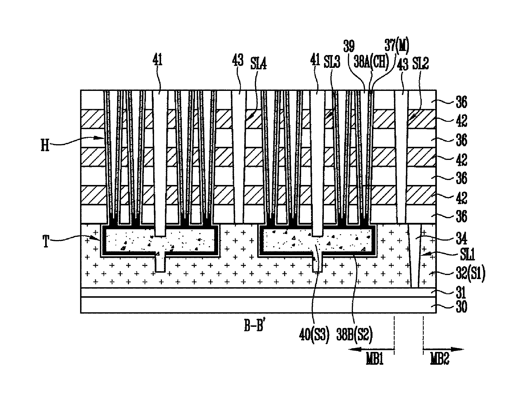
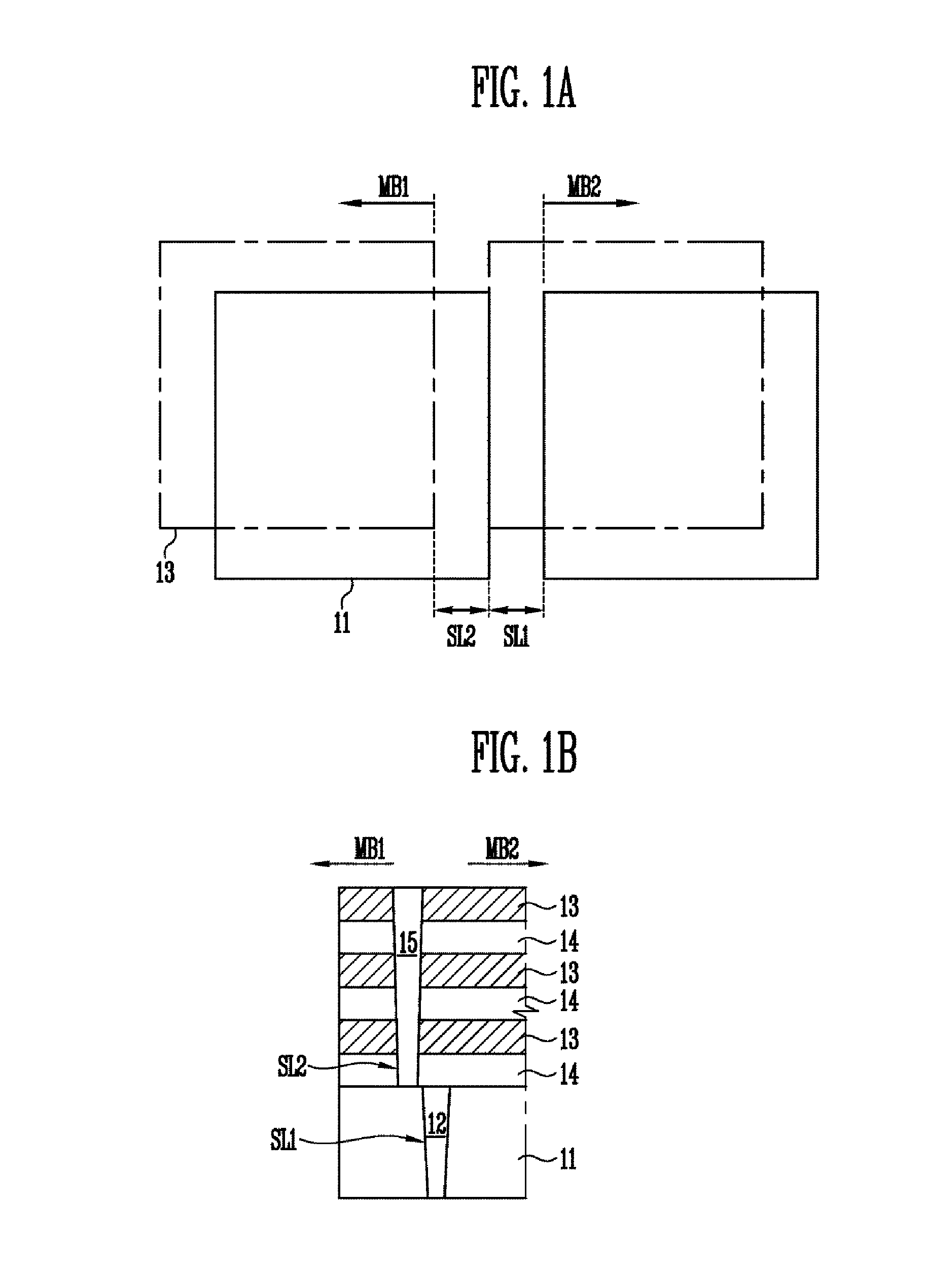
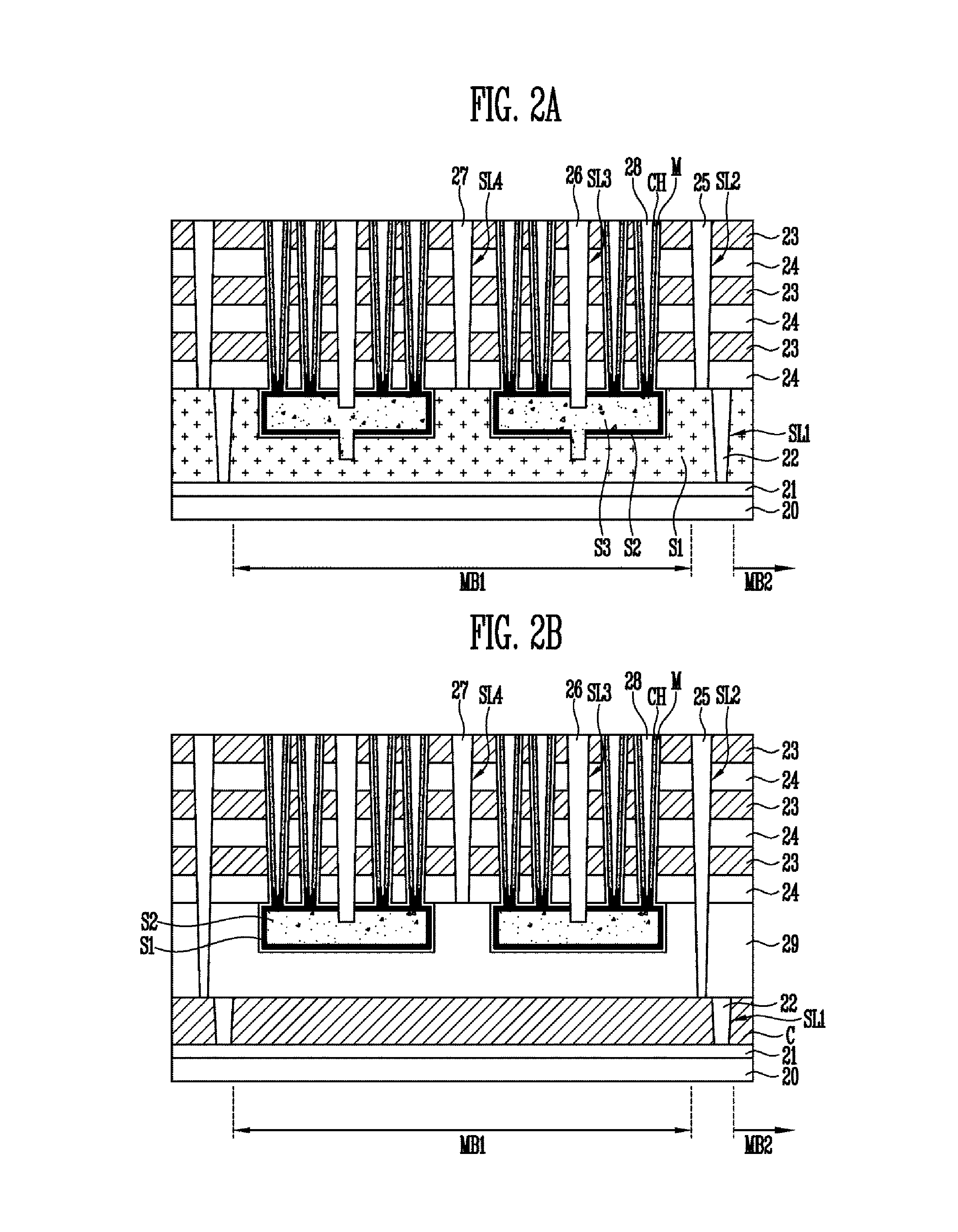
[0024]FIG. 1A and FIG. 1B are views illustrating a layout and a cross-section of a semiconductor device according to an embodiment of the present invention. FIG. 1A shows only the boundary between adjoining memory blocks for convenience of description.
[0025]In FIG. 1A and FIG. 1B, a semiconductor device of the present embodiments may include a first conductive layer 11 and second conductive layers 13 and interlayer dielectric layers 14 stacked in turn. Additionally, the semiconductor device may further include at least one first slit SL1 for...
PUM
 Abstract
Description
Claims
Application Information