Manufacturing method for edge illuminated type photodiode and semiconductor wafer

a manufacturing method and semiconductor technology, applied in the direction of photovoltaic energy generation, electrical apparatus, semiconductor devices, etc., can solve the problems of difficult to detect light in a relatively short wavelength region, contribution to output, and difficult to manufacture photodiodes described in the above applications, so as to prevent deformation and damage ensure the mechanical strength and facilitate the handling of the semiconductor wafer

Active Publication Date: 2015-03-31
HAMAMATSU PHOTONICS KK
View PDF3 Cites 1 Cited by
  • Summary
  • Abstract
  • Description
  • Claims
  • Application Information

AI Technical Summary

Benefits of technology

[0012]When the light in the relatively short wavelength region is incident through the side face into the edge illuminated type photodiode obtained by the present invention, the incident light is absorbed in the region near the side face to generate carriers. Since the side face serving as an incident surface (light receiving surface) is smooth, the carriers are less likely to be trapped in the side face (and the region near the side face), suppressing recombination of the generated carriers. Therefore, the generated carriers are prevented from undergoing extinction and thus make efficient contribution to output of the photodiode. As a result, the edge illuminated type photodiode obtained by the present invention can successfully detect the light in the relatively short wavelength region.
[0026]The trench may be formed for each corresponding device forming region so as to be physically separated from other trenches. In this case, the mechanical strength of the semiconductor wafer in which the trenches are formed is further ensured. Therefore, it becomes extremely easier to handle the semiconductor wafer and feasible to securely prevent the deformation and damage of the semiconductor wafer.

Problems solved by technology

The photodiodes described in the foregoing applications have the problem that it is hard for them to detect light in a relatively short wavelength region (e.g., the wavelength region of not more than 900 nm).
However, since the carriers are generated in the region near the side face, the generated carriers are trapped by the lattice defects of the side face to undergo recombination and extinction, making no contribution to output.
Therefore, it is difficult for the photodiodes described in the above applications to detect the light in the relatively short wavelength region.
As described above, the surface of the side face, if formed by dicing, is very rough, and the side face and the region near the side face in the photodiode tend to have defects.

Method used


Image

  • Manufacturing method for edge illuminated type photodiode and semiconductor wafer
  • Manufacturing method for edge illuminated type photodiode and semiconductor wafer
  • Manufacturing method for edge illuminated type photodiode and semiconductor wafer

Examples


first embodiment

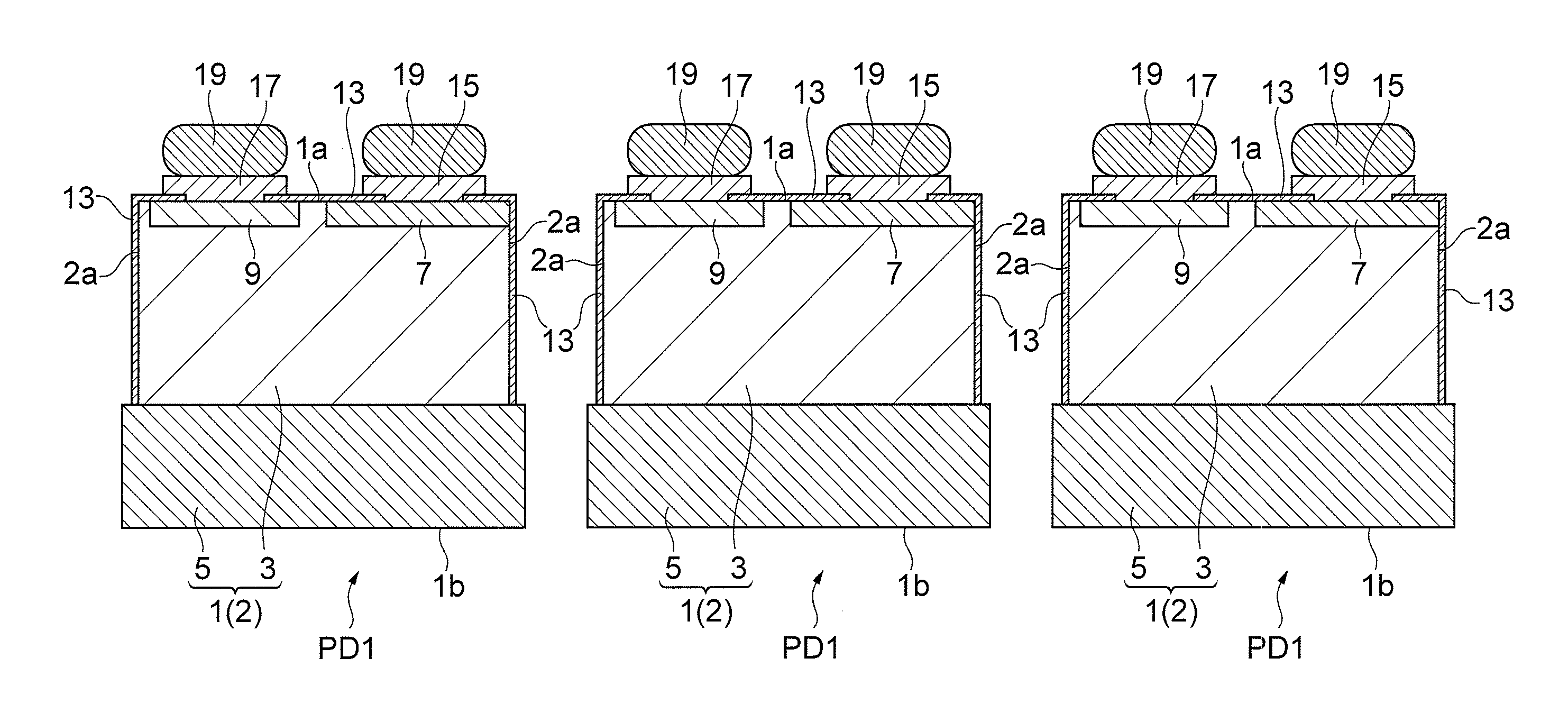
[0059]A manufacturing process for edge illuminated type photodiodes according to the first embodiment will be described with reference to FIGS. 1 to 13. FIGS. 1 to 13 are drawings for explaining the manufacturing process for edge illuminated type photodiodes according to the first embodiment.

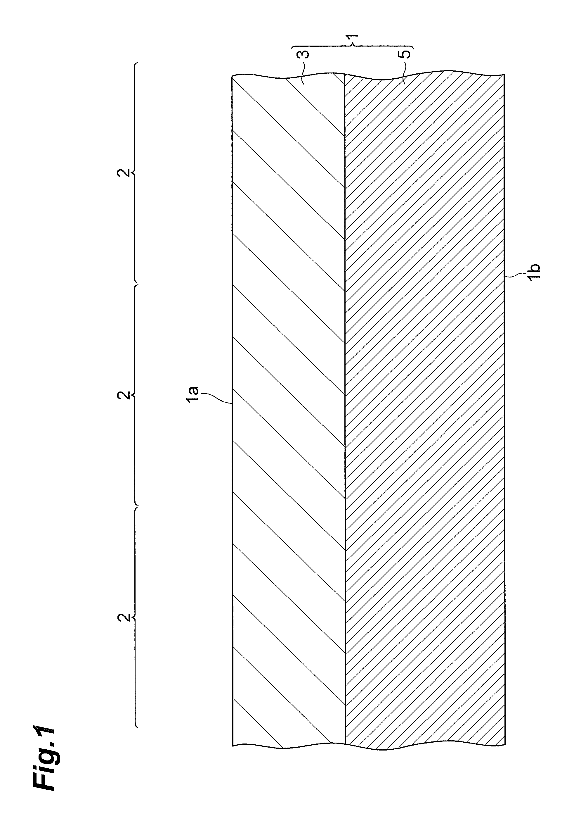
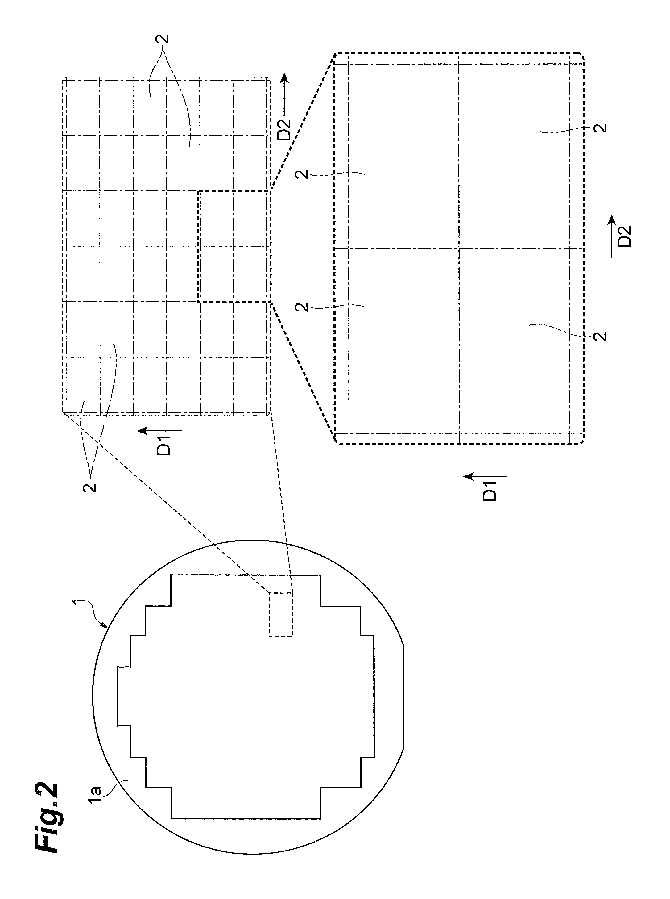
[0060]First, a semiconductor substrate 1 is prepared (cf. FIGS. 1 and 2). The semiconductor substrate 1 is a silicon substrate having a principal surface 1a and a principal surface 1b opposed to each other. The semiconductor substrate 1 includes a first substrate region 3 of the first conductivity type (e.g., n-type) located on the principal surface 1a side and a second substrate region 5 of the first conductivity type (e.g., n-type) located on the principal surface 1b side. The second substrate region 5 has a higher impurity concentration than the first substrate region 3.

[0061]The semiconductor substrate 1 can be obtained, for example, by growing on an n+-type semiconductor substrate with a hi...

second embodiment

[0100]A manufacturing process for edge illuminated type photodiodes according to the second embodiment will be described with reference to FIGS. 19 to 29. FIGS. 19 to 29 are drawings for explaining the manufacturing process for edge illuminated type photodiodes according to the second embodiment.

[0101]First, a semiconductor substrate 31 is prepared (cf. FIGS. 19 and 20). The semiconductor substrate 31 is a silicon substrate having a principal surface 31a and a principal surface 31b opposed to each other. The semiconductor substrate 31 includes a first substrate region 33 of the second conductivity type (e.g., p-type) located on the principal surface 31a side and a second substrate region 35 of the first conductivity type (e.g., n-type) located on the principal surface 31b side. The second substrate region 35 has a higher impurity concentration than the first substrate region 33.

[0102]The semiconductor substrate 31 can be obtained, for example, by growing on an n+-type semiconductor ...


PUM


Abstract

A manufacturing method for an edge illuminated type photodiode has: a process of forming an impurity-doped layer of a first conductivity type in each of device forming regions in a semiconductor substrate; a process of forming an impurity-doped layer of a second conductivity type in each of the device forming regions; a process of forming a trench extending in a direction of thickness of the semiconductor substrate from a principal surface, at a position of a boundary between adjacent device forming regions, by etching to expose side faces of the device forming regions; a process of forming an insulating film on the exposed side faces of the device forming regions; a process of forming an electrode for each corresponding impurity-doped layer on the principal surface side of the semiconductor substrate; and a process of implementing singulation of the semiconductor substrate into the individual device forming regions.

Description

CROSS-REFERENCE TO RELATED APPLICATIONS[0001]This application is based upon and claims the benefit of priorities from U.S. Provisional application Ser. No. 61 / 694,921 filed on Aug. 30, 2012, and Japanese Patent Application No. 2012-189402 filed on Aug. 30, 2012, the entire contents of which are incorporated herein by reference.BACKGROUND OF THE INVENTION[0002]1. Field of the Invention[0003]The present invention relates to a manufacturing method for an edge illuminated type photodiode, and a semiconductor wafer for obtaining the edge illuminated type photodiode.[0004]2. Related Background Art[0005]There are known edge illuminated type photodiodes in which a side face extending between a pair of principal faces opposed to each other serves as a light incident surface (e.g., cf. Japanese Patent Applications Laid-open No. H08-018151 and No. 2009-212109).SUMMARY OF THE INVENTION[0006]The photodiodes described in the foregoing applications have the problem that it is hard for them to dete...

Claims


Application Information

Patent Timeline
Patent Type & Authority Patents(United States)
IPC IPC(8): H01L21/00H01L31/0224H01L31/0232H01L31/0352H01L31/103H01L31/18
CPCH01L31/02327H01L31/022408H01L31/0352H01L31/03529H01L31/103H01L31/18H01L2224/11H01L27/1446H01L27/14603H01L27/1463H01L27/14632Y02E10/50
Inventor OGURI, HIROSHIISHIKAWA, YOSHITAKASAKAMOTO, AKIRATAGUCHI, TOMOYAFUJII, YOSHIMARO
Owner HAMAMATSU PHOTONICS KK
Why Eureka
Try Eureka