Diode structure and method for wire-last nanomesh technologies

a technology of nanomesh and diodes, applied in the direction of diodes, semiconductor devices, electrical equipment, etc., can solve the problems of increasing the use of non-planar devices in future cmos technologies, and achieve the effect of improving the use rate of non-planar devices

Active Publication Date: 2015-03-31
GLOBALFOUNDRIES U S INC
View PDF35 Cites 6 Cited by
  • Summary
  • Abstract
  • Description
  • Claims
  • Application Information

AI Technical Summary

Problems solved by technology

However, the use of non-planar devices in future CMOS technologies is becoming increasingly more pervasive.
One key issue in the use of these devices is other critical technology elements, such as diodes.

Method used


Image

  • Diode structure and method for wire-last nanomesh technologies
  • Diode structure and method for wire-last nanomesh technologies
  • Diode structure and method for wire-last nanomesh technologies

Examples


Embodiment Construction

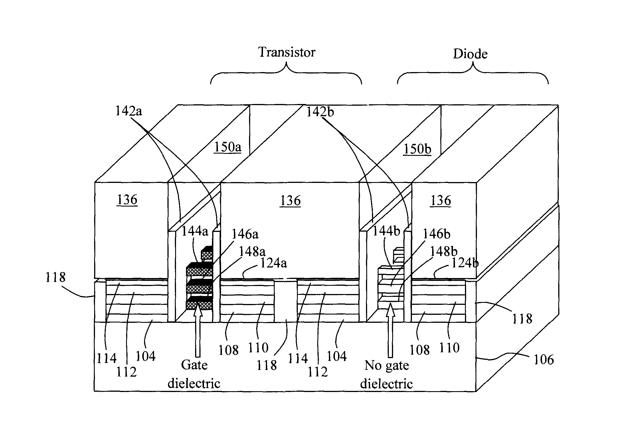
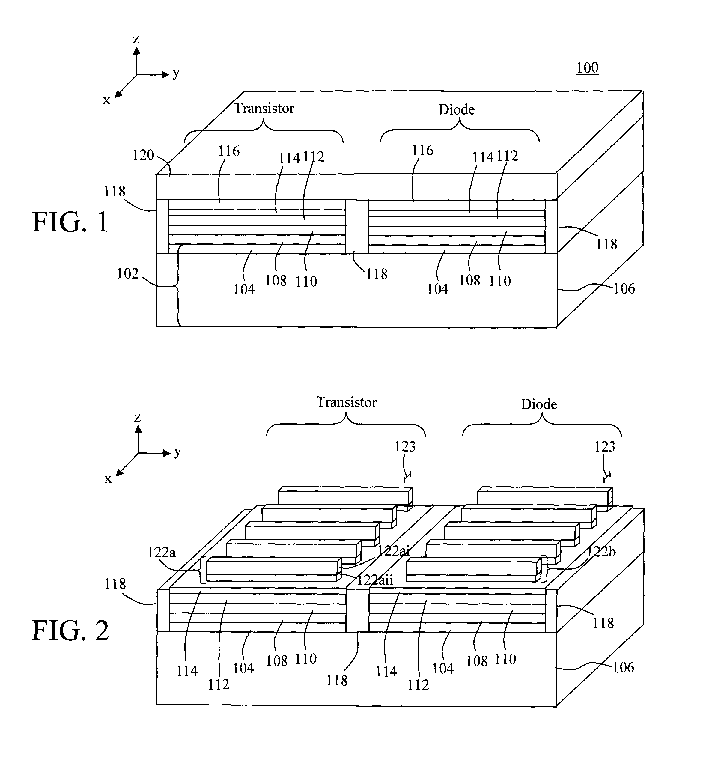
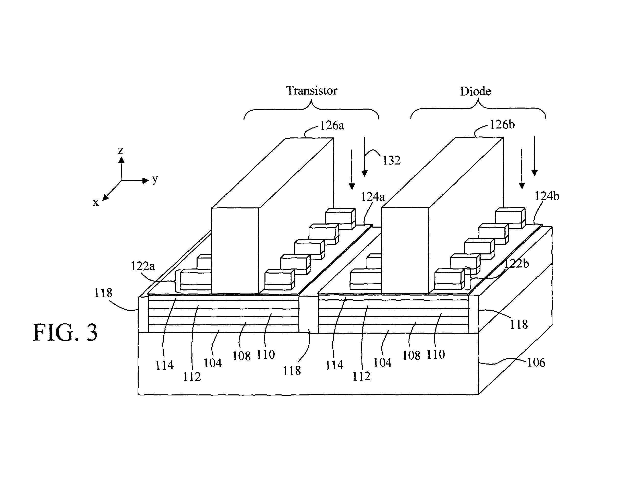
[0024]Provided herein are techniques for fabricating diodes in nanomesh-based devices. Techniques for fabricating diodes in FINFET devices are described for example in U.S. patent application Ser. No. 13 / 761,430, filed on Feb. 7, 2013, entitled “Diode Structure and Method for FINFET Technologies,” the contents of which are incorporated by reference herein. Techniques for fabricating diodes in gate-all-around nanowire devices are described for example in U.S. patent application Ser. No. 13 / 761,453, filed on Feb. 7, 2013, entitled “Diode Structure and Method for Gate All Around Silicon Nanowire Technologies,” the contents of which are incorporated by reference herein.

[0025]The present techniques assume a replacement gate fabrication process flow (also referred to herein as a “gate-last” approach). As will be apparent from the following description, in a replacement gate or gate-last approach, a dummy gate is formed and then replaced later in the process with a permanent, replacement g...


PUM


Abstract

In one aspect, a method of fabricating an electronic device includes the following steps. An alternating series of device and sacrificial layers are formed in a stack on an SOI wafer. Nanowire bars are etched into the device / sacrificial layers such that each of the device layers in a first portion of the stack and each of the device layers in a second portion of the stack has a source region, a drain region and a plurality of nanowire channels connecting the source region and the drain region. The sacrificial layers are removed from between the nanowire bars. A conformal gate dielectric layer is selectively formed surrounding the nanowire channels in the first portion of the stack which serve as a channel region of a nanomesh FET transistor. Gates are formed surrounding the nanowire channels in the first and second portions of the stack.

Description

CROSS-REFERENCE TO RELATED APPLICATION(S)[0001]This application is a continuation of U.S. application Ser. No. 13 / 761,476 filed on Feb. 7, 2013, the disclosure of which is incorporated by reference herein.FIELD OF THE INVENTION[0002]The present invention relates to nanomesh field-effect transistor (FET)-based electronic devices, and more particularly, to techniques for fabricating nanomesh FET diode devices.BACKGROUND OF THE INVENTION[0003]Non-transistor field effect transistor (FET) elements, such as capacitors and diodes are important elements in complementary metal-oxide semiconductor (CMOS) technology. Much research has been done regarding planar diode and capacitor device structures. See, for example, U.S. Patent Application Publication Number 2011 / 0108900 A1 filed by Chang et al., entitled “Bi-Directional Self-Aligned FET Capacitor.”[0004]However, the use of non-planar devices in future CMOS technologies is becoming increasingly more pervasive. One key issue in the use of thes...

Claims


Application Information

Patent Timeline
Patent Type & Authority Patents(United States)
IPC IPC(8): H01L27/12B82Y99/00H01L29/66H01L29/78
CPCH01L27/1203H01L29/66477H01L29/78B82Y99/00Y10S977/762B82Y10/00B82Y40/00H01L27/0629H01L29/0673H01L29/16H01L29/42392H01L29/66136H01L29/66439H01L29/775H01L29/78696H01L29/861Y10S977/938
Inventor CHANG, JOSEPHINE B.LAUER, ISAACLIN, CHUNG-HSUNSLEIGHT, JEFFREY W.
Owner GLOBALFOUNDRIES U S INC
Why Eureka
Try Eureka