
Semiconductor device

a technology of semiconductor devices and semiconductors, applied in semiconductor devices, semiconductor/solid-state device details, electrical apparatus, etc., can solve the problems of significant difficulty in defining practically impossible to quantify the dependence of esd tolerance on the layout of nmos transistors, etc., to achieve the effect of increasing the esd tolerance of semiconductor devices

Active Publication Date: 2015-04-14
ABLIC INC
View PDF2 Cites 1 Cited by
  • Summary
  • Abstract
  • Description
  • Claims
  • Application Information

AI Technical Summary

Benefits of technology

This patent describes a method of improving the ability of a semiconductor device to withstand Electrostatic Discharge (ESD) events. It does this by using a special circuit design that allows for uniform operation of the different channels in the device, which increases its overall tolerance to ESD. This is achieved by creating a via that connects the pad to the drain of a specific transistor, which results in a more uniform distribution of current in the event of a surge.

Problems solved by technology

However it is significantly difficult to define the layout of the NMOS transistor based on the surge current since a surge current caused by ESD is an extremely large and instantaneous.
In contrast, it is practically almost impossible to quantify the dependency of the ESD tolerance on the layout of the NMOS transistor, either.

Method used


Image

  • Semiconductor device
  • Semiconductor device
  • Semiconductor device

Examples


first embodiment

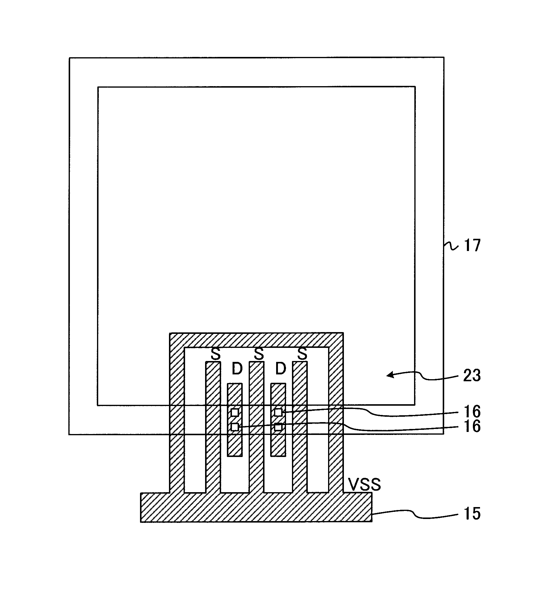
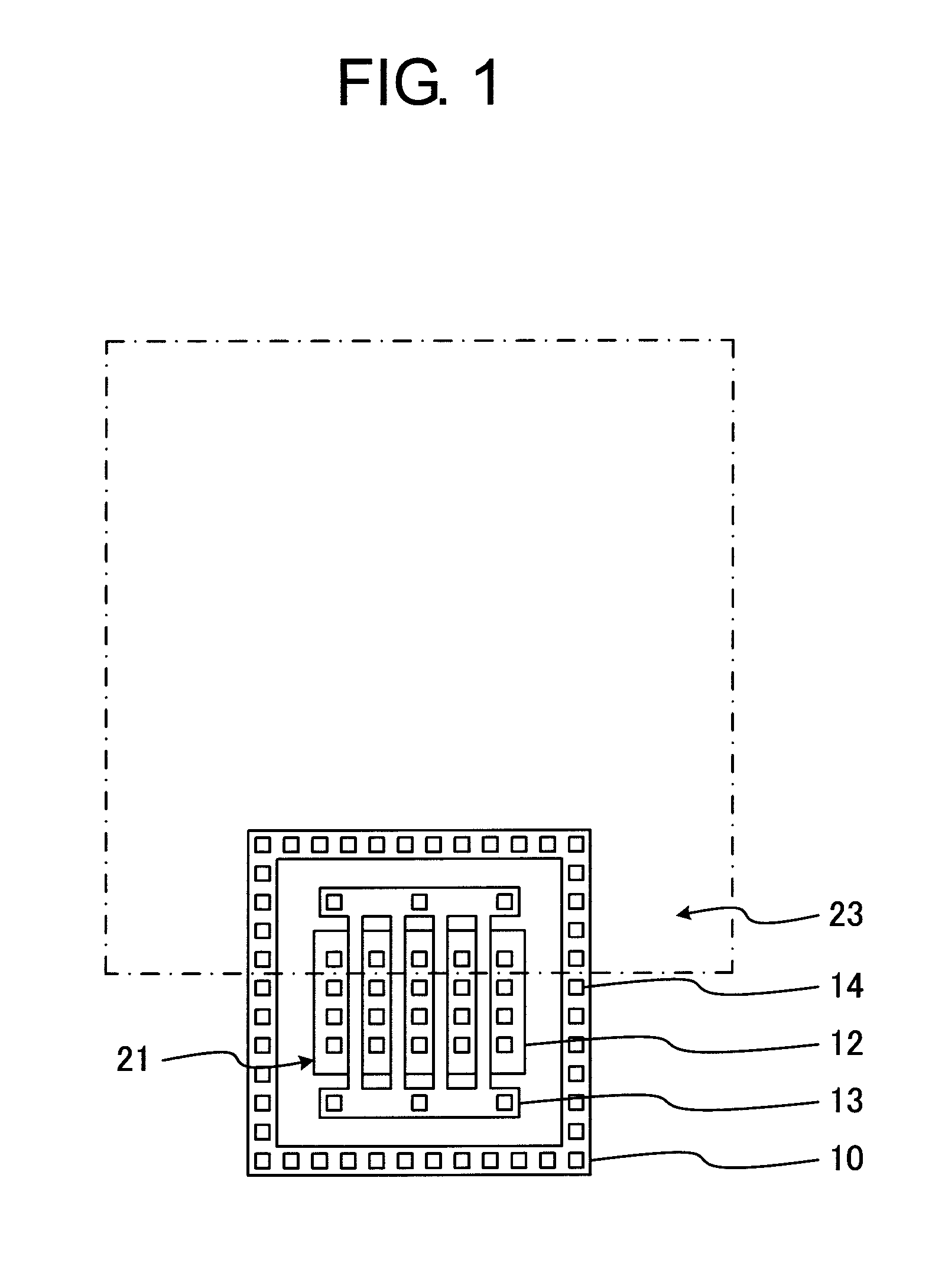
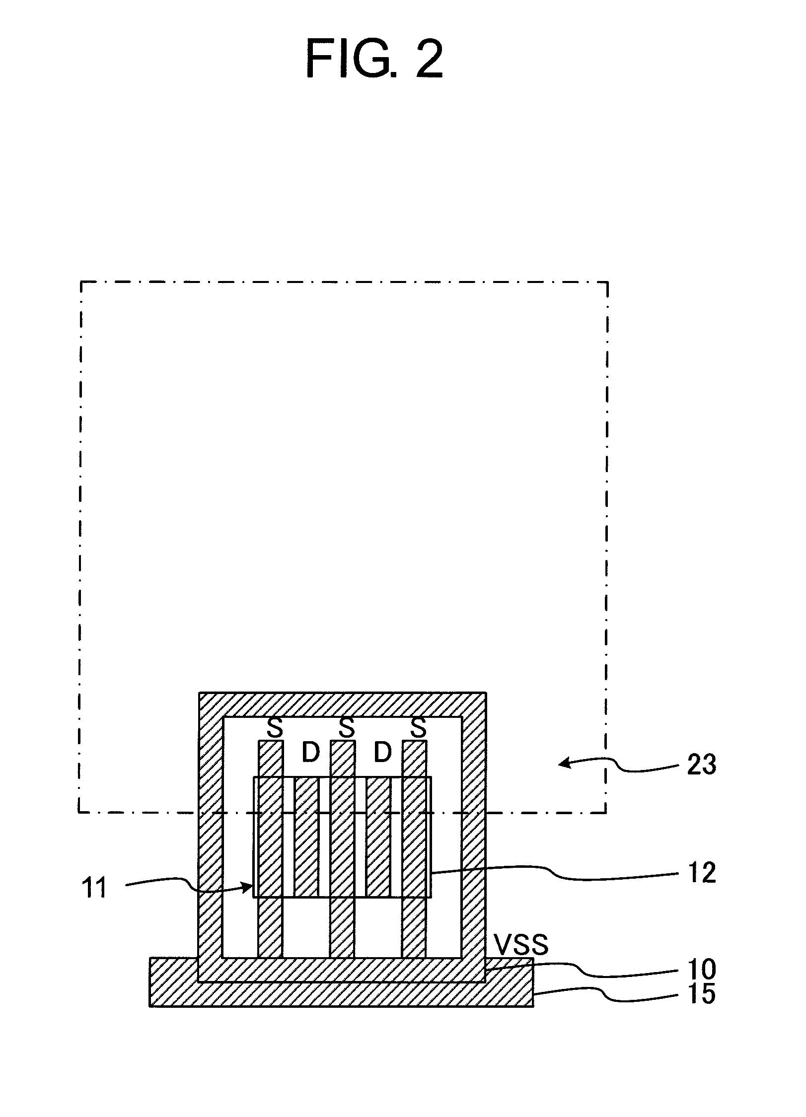
[0023]First, a pad structure of a semiconductor device according to the present invention is described with reference to plan views of FIGS. 1 to 4, which illustrate the pad structure of the semiconductor device. FIG. 1 illustrates diffusion regions, a gate electrode, a contact, and a pad opening. FIG. 2 illustrates the diffusion regions, a lower metal film, and the pad opening. FIG. 3 illustrates the lower metal film, a first via, an intermediate metal film, and the pad opening. FIG. 4 illustrates a second via, an upper metal film, and the pad opening.

[0024]As illustrated in FIG. 1, a gate electrode 13, a P-type diffusion region 10 for fixing a substrate potential, and an N-type diffusion region 12 for a source and a drain are arranged so as to overlap with an edge of a pad opening 23, to thereby construct an NMOS transistor 21. The NMOS transistor 21 is a multi-finger transistor, which is surrounded by the P-type diffusion region 10, and includes the N-type diffusion regions 12 fo...

second embodiment

[0035]FIG. 6 illustrates the present invention. FIG. 6 illustrates a diffusion region, a gate electrode, a contact, and a pad opening. In the case where the NMOS transistor 21 has the source regions at both ends and at the center, in order to stabilize a substrate potential in the vicinity of the source and drain regions, the P-type diffusion region 10 for fixing the substrate potential can be arranged along the center of the NMOS transistor 21 so as to be adjacent to the N-type diffusion region 12 for the source.

third embodiment

[0036]FIG. 7 illustrates the present invention. FIG. 7 illustrates a diffusion region, a gate electrode, a contact, and a pad opening. Although the NMOS transistor 21 of FIG. 1 includes the N-type diffusion region 12 serving as the source as a diffusion region at the end in the gate length direction, the NMOS transistor 21 may include an N-type diffusion region 12 serving as the drain as illustrated in FIG. 7. In FIG. 7, the location of the N-type diffusion region 12 for the source is changed, and along therewith, the location of the contact 14 on the gate electrode 13 is also changed.

[0037]As illustrated in FIG. 8, two NMOS transistors 21 may be arranged so as to be opposed to each other. In this case, the first via 16 for one of the NMOS transistors 21 is arranged on one side of the intermediate metal film 17, and the first via 16 for the other of the NMOS transistors 21 is arranged on another side thereof opposed to the one side. In this manner, the symmetry is ensured.

[0038]As i...


PUM


Abstract

Provided is a semiconductor device having high ESD tolerance. A first via (16) is used for electrically connecting a pad to a drain of an NMOS transistor of an ESD protection circuit. The first via (16) is arranged directly above the drain and present substantially directly under the pad. Consequently, a surge current caused by ESD and applied to the pad is more likely to flow uniformly among all the drains. Then, respective channels of the NMOS transistor of the ESD protection circuit are more likely to uniformly operate, and hence the ESD tolerance of the semiconductor device increases.

Description

BACKGROUND OF THE INVENTION[0001]1. Field of the Invention[0002]The present invention relates to a semiconductor device including an NMOS transistor under a pad.[0003]2. Description of the Related Art[0004]A semiconductor device, also called an IC or a semiconductor chip, has a pad as an external connection electrode in order to establish an electrical connection to another element or another semiconductor device. In the vicinity of the pad, an ESD protection circuit is generally provided for protecting an internal circuit of the semiconductor device from electrostatic discharge (ESD). The ESD protection circuit uses a multi-finger NMOS transistor in many cases. In this NMOS transistor, a gate electrode, a source, and a terminal for applying a substrate potential are connected to a ground terminal, and a drain is connected to the pad.[0005]Various possible approaches are attempted for the ESD protection circuit using the multi-finger NMOS transistor so that respective channels may u...

Claims


Application Information

Patent Timeline
Patent Type & Authority Patents(United States)
IPC IPC(8): H01L23/62H01L29/76H01L23/482H01L27/02H01L29/06H01L29/417H01L29/423
CPCH01L27/0266H01L29/41758H01L29/4238H01L29/0692H01L23/4824H01L27/0274H01L2924/0002H01L2924/00H01L27/04
Inventor KOYAMA, TAKESHIHIROSE, YOSHITSUGU
Owner ABLIC INC
Learn More