Memory circuit and memory device

a memory circuit and memory technology, applied in the field of memory circuits, can solve the problems of large power consumption of conventional memory circuits, increased power consumption, and loss of stored data, and achieve the effect of suppressing the current flow of the memory circuit and reducing power consumption

Active Publication Date: 2015-04-14
SEMICON ENERGY LAB CO LTD
View PDF143 Cites 0 Cited by
  • Summary
  • Abstract
  • Description
  • Claims
  • Application Information

AI Technical Summary

Benefits of technology

[0013]An object of one embodiment of the present invention is to reduce power consumption.
[0014]In one embodiment of the present invention, a memory circuit is constituted using an inverter composed of two field-effect transistors having the same conductivity type. One of the two field-effect transistors is a field-effect transistor in which the amount of current between a source and a drain is changed in response to a control signal. The above structure can reduce the leakage current in a hold period, for example.
[0017]According to one embodiment of the present invention, unwanted current flow in the memory circuit can be suppressed, so that power consumption can be reduced.

Problems solved by technology

A conventional memory circuit has a problem of large power consumption.
As a result, power consumption is increased as the capacity of the SRAM is increased, for example.
Moreover, in the memory circuit disclosed in Patent Document 1, stored data is lost when supply of the power supply voltage stops.
Accordingly, the power supply voltage needs to continue to be supplied at all times while data is held, which increases power consumption.

Method used


Image

  • Memory circuit and memory device
  • Memory circuit and memory device
  • Memory circuit and memory device

Examples


embodiment 1

[0035]In this embodiment, an example of a memory circuit including an inverter composed of only transistors having the same conductivity type will be described with reference to FIGS. 1A, 1B, 1C1, and 1C2, FIG. 2, and FIGS. 3A and 3B.

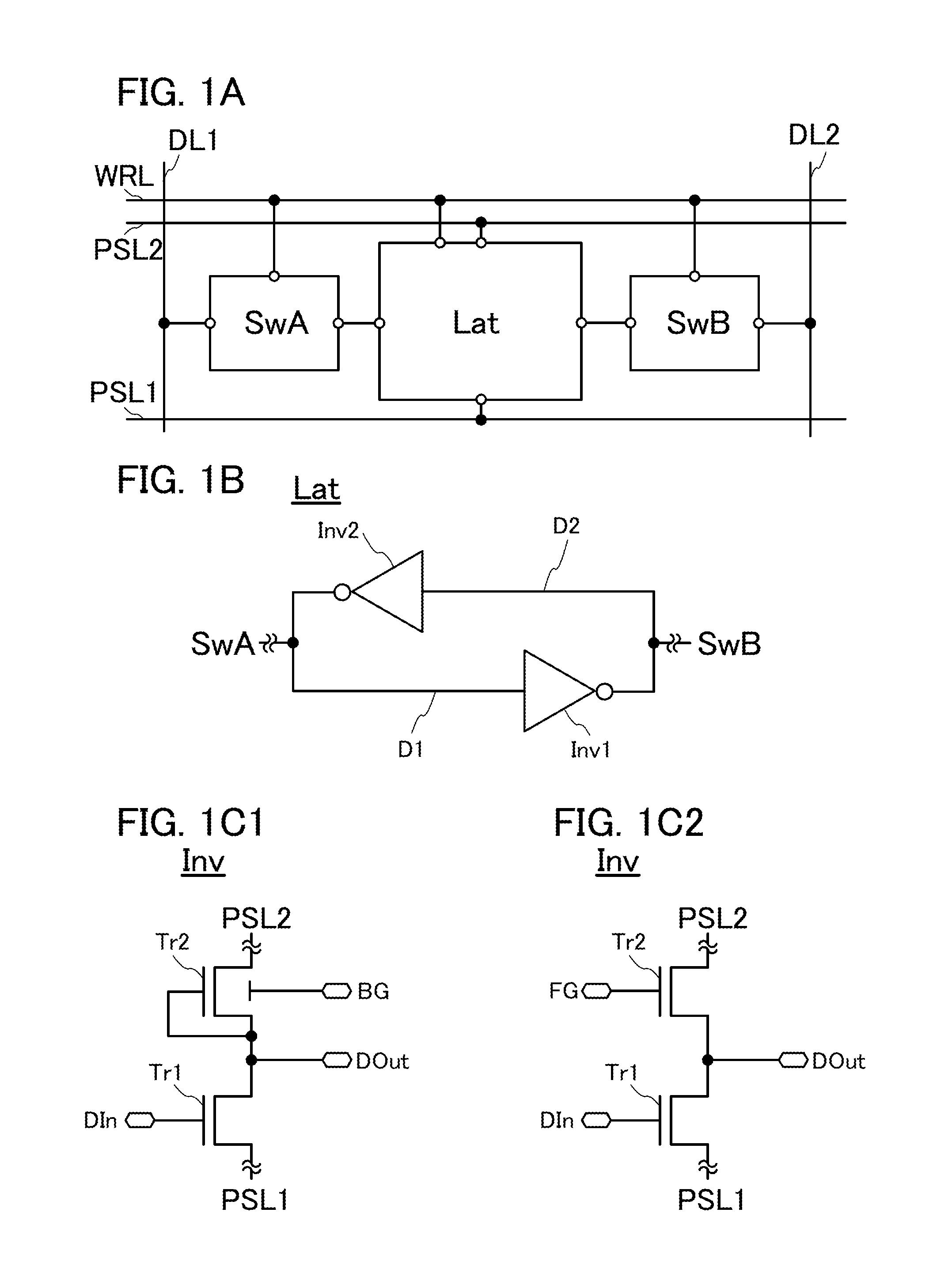
[0036]The memory circuit in this embodiment includes a latch unit Lat, a switch unit SwA, and a switch unit SwB, for example, as illustrated in FIG. 1A.

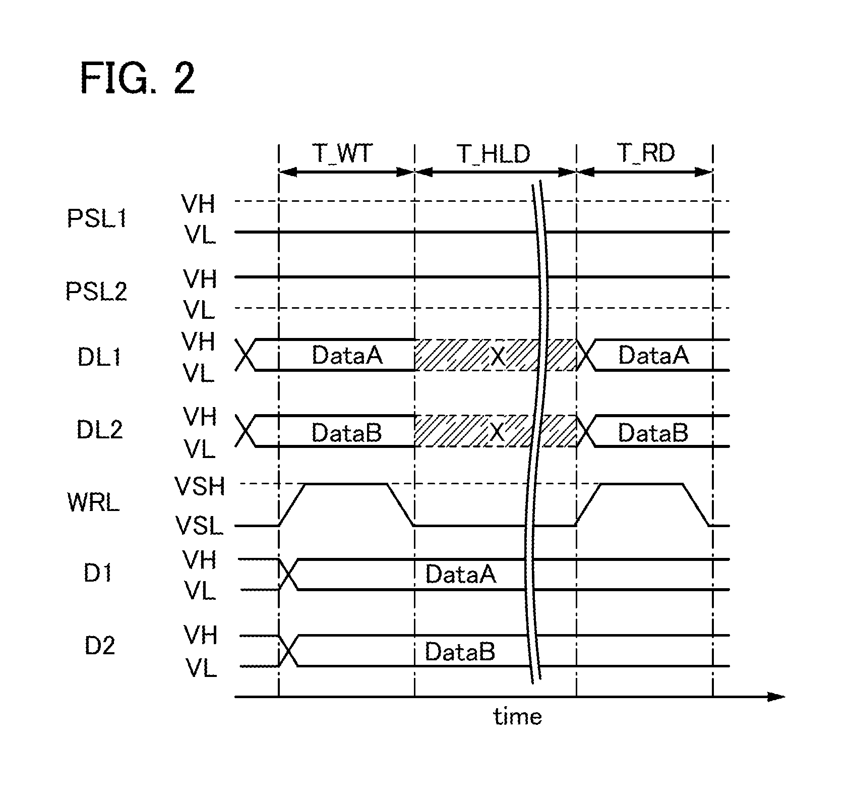
[0037]The latch unit Lat is supplied with the power supply voltage through a first power supply line PSL1 and a second power supply line PSL2. The latch unit Lat is also supplied with a control signal WR through a rewrite / read control signal line WRL. The latch unit Lat has a function of storing first data D1 and second data D2. The first data D1 and the second data D2 are rewritten and read in accordance with the control signal WR.

[0038]The switch unit SwA and the switch unit SwB are supplied with the control signal WR through the rewrite / read control signal line WRL.

[0039]The switch unit SwA has a func...

embodiment 2

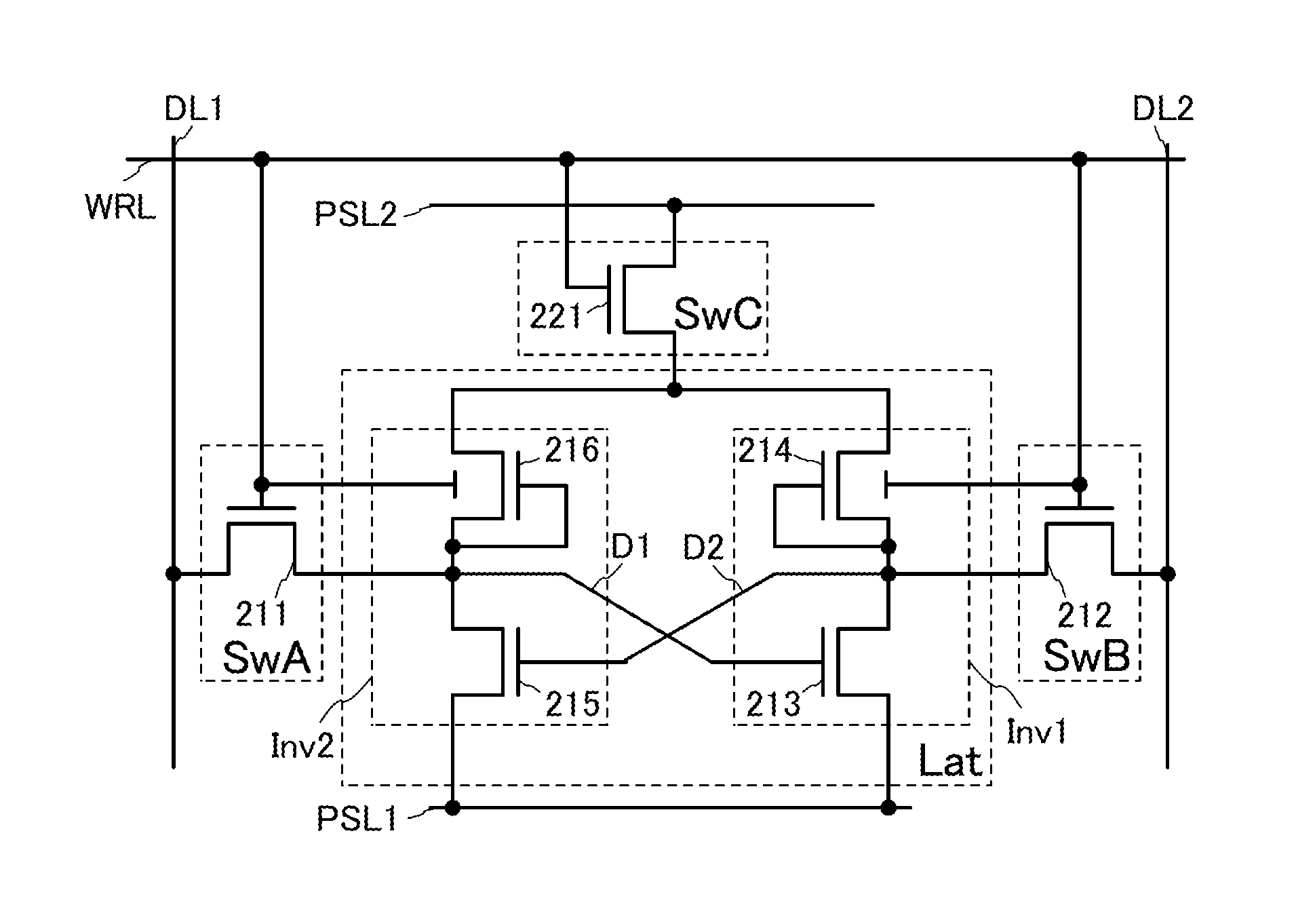
[0085]In this embodiment, as a specific example of the memory circuit described in Embodiment 1, a memory circuit constituted only of n-channel field-effect transistors will be described with reference to FIGS. 4A and 4B, FIGS. 5A and 5B, FIGS. 6A and 6B, FIGS. 7A and 7B, and FIG. 8. Note that the description of the memory circuit in Embodiment 1 can apply to the same portions as in Embodiment 1 as appropriate.

[0086]FIG. 4A illustrates an example of a memory circuit in this embodiment. The memory circuit illustrated in FIG. 4A includes the latch unit Lat, the switch unit SwA, and the switch unit SwB.

[0087]The switch unit SwA has a field-effect transistor 211.

[0088]One of a source and a drain of the field-effect transistor 211 is electrically connected to the first data signal line DL1. A gate of the field-effect transistor 211 is electrically connected to the rewrite / read control signal line WRL.

[0089]The switch unit SwB has a field-effect transistor 212.

[0090]One of a source and a ...

embodiment 3

[0137]In this embodiment, an example of the structure of the memory circuit described in Embodiment 2 will be described with reference to FIGS. 9A to 9C. FIGS. 9A to 9C are schematic cross-sectional views.

[0138]As illustrated in FIGS. 9A to 9C, a memory circuit according to one example of this embodiment has a structure in which field-effect transistors 701 and 702 included in the first inverter Inv1 or the second inverter Inv2 are stacked over a field-effect transistor 700 provided in the switch unit SwA or the switch unit SwB. The field-effect transistors 700 to 702 have the same conductivity type. The field-effect transistor 701 has a pair of gates. Here, one of the pair of gates is called a first gate and the other thereof is called a second gate. Note that the structures of the field-effect transistors 700 to 702 are not limited to those illustrated in FIGS. 9A to 9C.

[0139]The memory circuit illustrated in FIGS. 9A to 9C includes an insulating layer 711, a semiconductor layer 7...


PUM


Abstract

To reduce power consumption, a memory circuit includes a latch unit in which first data and second data are rewritten and read in accordance with a control signal, a first switch unit that controls rewrite and read of the first data stored in the latch unit by being turned on or off in response to the control signal, and a second switch unit that controls rewrite and read of the second data stored in the latch unit by being turned on or off in response to the control signal. The latch unit includes a first inverter and a second inverter. At least one of the first inverter and the second inverter includes a first field-effect transistor, and a second field-effect transistor that has the same conductivity type as the first field-effect transistor and has a gate potential controlled in accordance with the control signal.

Description

BACKGROUND OF THE INVENTION[0001]1. Field of the Invention[0002]One embodiment of the present invention relates to a memory circuit. Further, one embodiment of the present invention relates to a memory device including a memory circuit.[0003]2. Description of the Related Art[0004]In recent years, devices including circuits composed of only transistors having the same conductivity type (also referred to as circuits composed of only n-channel transistors or p-channel transistors) have been developed.[0005]An example of the circuit composed of only transistors having the same conductivity type is an inverter, which is a logic gate.[0006]For example, when the mobility is very different between a p-channel transistor and an n-channel transistor that both include a channel formation region containing the same semiconductor material, it is difficult to constitute an inverter using these p-channel and n-channel transistors. In contrast, an inverter can be easily constituted of transistors h...

Claims


Application Information

Patent Timeline
Patent Type & Authority Patents(United States)
IPC IPC(8): G11C11/00G11C7/12G11C11/412G11C11/419
CPCG11C7/12G11C11/412G11C11/419G11C11/00
Inventor OHMARU, TAKURO
Owner SEMICON ENERGY LAB CO LTD
Why Eureka
Try Eureka