Printed antennas, methods of printing an antenna, and devices including the printed antenna

a technology of printed antennas and antennas, applied in the direction of antennas, instruments, antenna details, etc., can solve the problems of increasing costs, reducing the efficiency of material utilization, and reducing the size of dies, so as to reduce the cost of processing equipment, reduce the cost of processing, and eliminate the effect of expensive subtractive steps

Inactive Publication Date: 2015-04-28
ENSURGE MICROPOWER ASA
View PDF92 Cites 4 Cited by
  • Summary
  • Abstract
  • Description
  • Claims
  • Application Information

AI Technical Summary

Benefits of technology

[0017]Various embodiments of the present invention relate to printed wireless integrated circuits (e.g., sensors, displays, tags having one or more RF, HF, VHF, UHF, and / or electronic article surveillance [EAS] functions, and other articles of manufacture that send and / or receive wireless signals, etc.). Printing has potential cost advantages for manufacturing such integrated circuits, since printing increases the efficiency of materials utilization (e.g., by additive or semi-additive processing), combines deposition and patterning steps eliminating expensive subtractive step in conventional processing, and leverages low capital expenditures and operating costs for processing equipment. The materials efficiency and additive processing enable a lower cost per unit area for the processed carriers, as well as low cost attach processing and / or integration of passive devices with the active circuitry. Furthermore, high throughput conventional printing processes can be adapted to flexible substrates (e.g., a plastic sheet or a metal foil), thereby improving and / or expanding uses of wireless devices in a number of applications. Also, maskless processes such as printing enable facile customization of devices (e.g., wireless RF), for example where each individual RF device is provided with a unique identification code and / or a unique response time delay with respect to a reader inquiry. Furthermore, if an antenna can be printed in a manner that facilitates the direct placement of the printed antenna on an integrated circuit and / or a substrate containing the integrated circuit, the cost of the antenna “attach” process can be reduced significantly.
[0018]The use of printing technology and ink facilitates the manufacturing of a low cost, but relatively large, printed integrated circuit (PIC). To improve yield and / or further reduce cost, at least part of an antenna or antenna precursor layer can be printed directly onto the printed integrated circuit and / or the substrate on which the printed integrated circuit is formed. Thus, the integrated circuit and the antenna can, in effect, directly contact each other, eliminating the need for a conventional die attach process and / or a strap-to-antenna attach process by which the integrated circuit (on a strap) is attached to the antenna (on a separate substrate).
[0019]By reducing the number of relatively expensive and / or low throughput attachment steps, as well as reducing the cost of fabricating the active electronics, a low cost wireless device may be produced by directly printing or otherwise forming an antenna on the integrated circuit and / or on the substrate. As a result, the present invention provides a relatively low-cost process for producing a wireless device, such as an RFID (or EAS) tag, comprising an integrated circuit and an antenna. These and other advantages of the present invention will become readily apparent from the detailed description of various embodiments below.

Problems solved by technology

The direct die attach process, an example of which is shown in FIGS. 1A-1B, is a relatively slow process, which can make it relatively expensive for a given throughput.
The size of the die is limited, and the relatively small die dimensions result in a need for higher accuracy pick and place systems, which further increases costs.
Also, the attach process often involves the use of heat, time, and / or UV exposure.
Manufacturing conventional RFID devices using the strap attach process also has cost limitations because the process inherently requires the same die attach process as the direct die-to-antenna attach process to place the die on the strap.
The strap attach process also introduces additional process steps, which result in lower yields and higher costs.
However, the cost of certain adhesives and / or of crimping or welding processes may still be higher than desired.
The high precision pick-and-place equipment has a relatively high capital cost and is typically slower than lower precision equipment.
As a result, the conventional attach process has a proportionately high cost relative to the overall manufacturing cost.
High RFID tag prices have been an obstacle against widespread adoption of RFID technology, especially in item-level retail applications and other low-cost, high-volume applications.

Method used


Image

  • Printed antennas, methods of printing an antenna, and devices including the printed antenna
  • Printed antennas, methods of printing an antenna, and devices including the printed antenna
  • Printed antennas, methods of printing an antenna, and devices including the printed antenna

Examples


Embodiment Construction

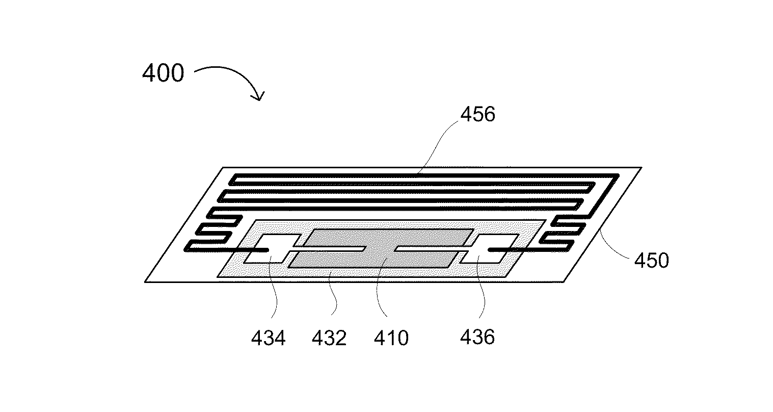
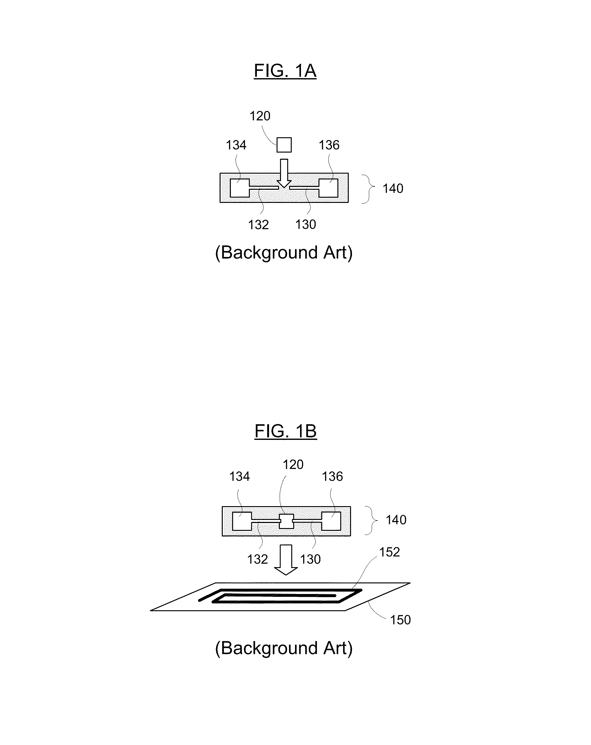
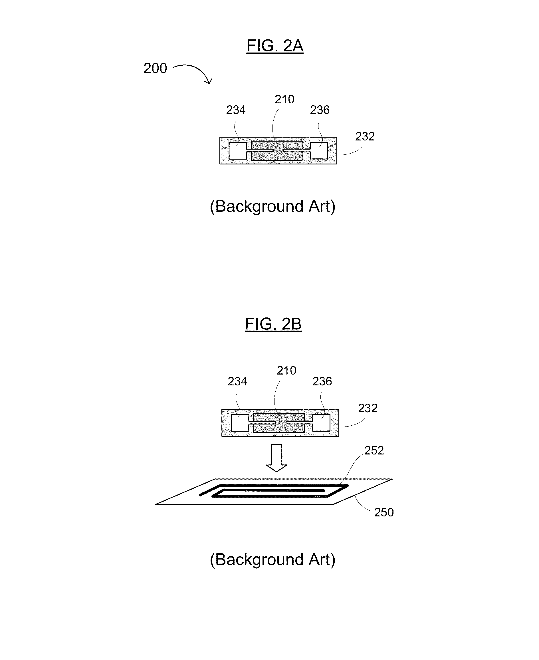
[0026]Reference will now be made in detail to certain embodiments of the invention, examples of which are illustrated in the accompanying drawings. While the invention will be described in conjunction with the disclosed embodiments, it will be understood that they are not intended to limit the invention to these embodiments. On the contrary, the invention is intended to cover alternatives, modifications and equivalents that may be included within the spirit and scope of the invention as defined by the appended claims. Furthermore, in the following detailed description, numerous specific details are set forth in order to provide a thorough understanding of the present invention. However, it will be readily apparent to one skilled in the art that the present invention may be practiced without these specific details. In other instances, well-known methods, procedures, components, and circuits have not been described in detail so as not to unnecessarily obscure aspects of the present in...


PUM

PropertyMeasurementUnit
temperatureaaaaaaaaaa

Abstract

Wireless devices such as sensors, interactive displays and electronic article surveillance (EAS) and / or radio frequency identification (RFID) tags including integrated circuitry and an antenna and / or inductor printed thereon, and methods for making and using the same, are disclosed. The device generally includes an integrated circuit on a substrate and an antenna, directly on the substrate and / or the integrated circuit, in electrical communication with the integrated circuit. The method of making a wireless device generally includes forming an integrated circuit on the substrate and printing at least part of an antenna or antenna precursor layer on the integrated circuit and / or substrate. The present invention advantageously provides a low cost wireless device capable of operating at MHz frequencies that can be manufactured in a shorter time period than conventional devices.

Description

RELATED APPLICATIONS[0001]This application claims the benefit of U.S. Provisional Patent Application No. 61 / 117,830, filed Nov. 25, 2008, which is incorporated herein by reference in its entirety.FIELD OF THE INVENTION[0002]The present invention generally relates to the field of wireless devices such as sensors and electronic article surveillance (EAS), radio frequency (RF) and / or identification (ID) tags. More specifically, embodiments of the present invention pertain to tags / devices utilizing an integrated circuit with an antenna printed thereon, and methods for their manufacturing and / or production.DISCUSSION OF THE BACKGROUND[0003]Remotely powered electronic devices and related systems are known. For example, U.S. Pat. No. 5,099,227, issued to Geiszler et al. and entitled “Proximity Detecting Apparatus,” discloses a remotely powered device which uses electromagnetic coupling to derive power from a remote source, then uses both electromagnetic and electrostatic coupling to transm...

Claims


Application Information

Patent Timeline
Patent Type & Authority Patents(United States)
IPC IPC(8): G06K19/06G06K19/077H01Q1/22H01Q7/00H01Q23/00
CPCH01Q7/00G06K19/07749H01Q1/2208H01Q1/2225H01Q23/00Y10T29/49018G06K19/07783
Inventor PAVATE, VIKRAMCHOI, CRISWELL
Owner ENSURGE MICROPOWER ASA
Why Eureka
Try Eureka