ZnO film structure and method of forming the same

a technology of zno film and structure, applied in the field of zno film, can solve the problems of difficult to form a zno single crystal, zno film is directly formed on the siosub>2 /sub>mask, low optical output, etc., and achieve the effect of reducing the reactivity to zno

Inactive Publication Date: 2015-04-28
GWANGJU INST OF SCI & TECH
View PDF1 Cites 0 Cited by
  • Summary
  • Abstract
  • Description
  • Claims
  • Application Information

AI Technical Summary

Benefits of technology

[0010]An object of the present invention is to provide a ZnO film structure using a mask capable of blocking progress of dislocation and having minimized reactivity to ZnO, and a method of forming the same.

Problems solved by technology

However, at the time of manufacturing a light emitting diode based on ZnO, there is a problem that an optical output is low.
On the other hand, in the case of growing the ZnO film using the SiO2 mask, a problem that the ZnO film is directly formed on the SiO2 mask occurs.
Therefore, it is difficult to form a ZnO single crystal and it is impossible to apply the ELOG technology.

Method used


Image

  • ZnO film structure and method of forming the same
  • ZnO film structure and method of forming the same
  • ZnO film structure and method of forming the same

Examples


preparation example

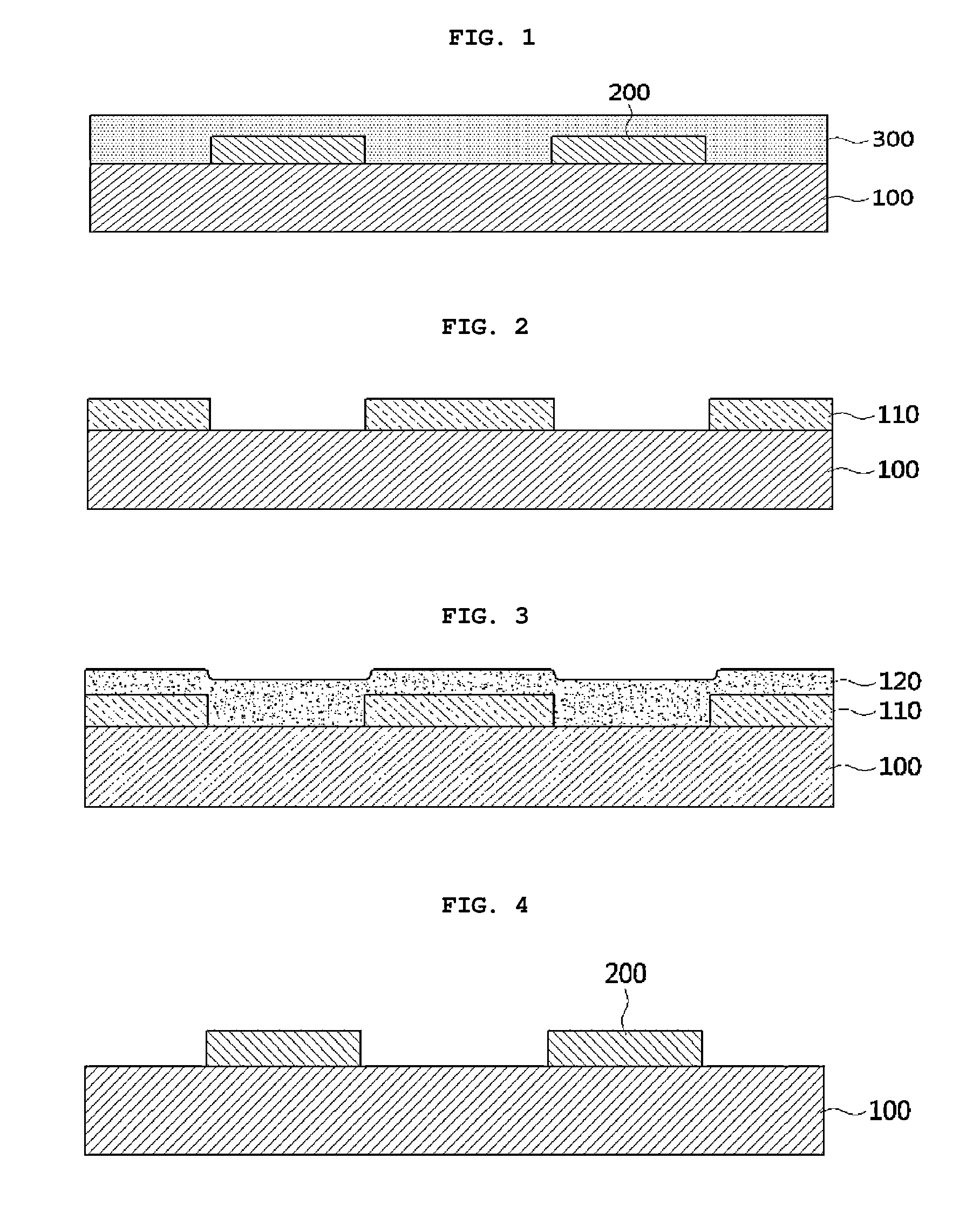
[0040]A sapphire substrate was prepared and MgF2 was used as a mask layer. First, a ZnO film was primarily formed on the sapphire substrate by a MOCVD process. The ZnO film is formed by a general MOCVD process. Mask layers having shapes of stripe patterns were formed on the ZnO film by a method of FIGS. 2 to 4. A preliminary mask layer was formed by an E-beam deposition process.

[0041]An interval between the stripe patterns of the mask layers is 6.5 μm.

[0042]Then, an ELOG process was performed. At the time of performing the ELOG process, a growth temperature is 750° C., DEZn is used as a zinc precursor, and a flow rate is set to 20.1 μmol / min. In addition, a flow rate of oxygen gas is set to 66,920 μmol / min. A mole ratio of O2 to DEZn is 3330.

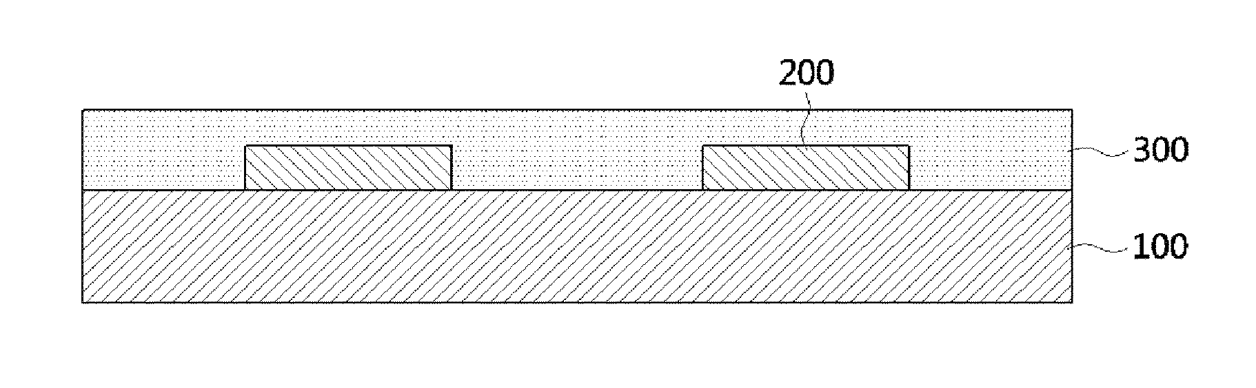
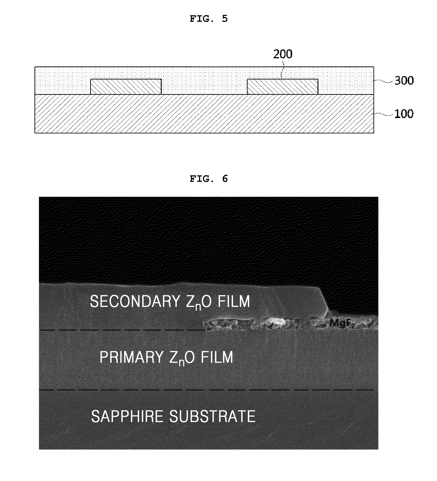
[0043]FIG. 6 is an image showing a ZnO film formed according to Preparation Example of the present exemplary embodiment.

[0044]Referring to FIG. 6, the ZnO film is primarily formed on the sapphire substrate. The primarily formed ZnO film has a th...


PUM

PropertyMeasurementUnit
melting pointaaaaaaaaaa
thicknessaaaaaaaaaa

Abstract

Disclosed herein are a ZnO film structure and a method of forming the same. Dislocation density of a ZnO film grown through epitaxial lateral overgrowth (ELOG) is minimized. In order to block a chemical reaction between the ZnO film and a mask layer at the time of performing the ELOG, a material of the mask layer is AlF3, NaF2, SrF, or MgF2. Therefore, the chemical reaction between ZnO and the mask layer is blocked and a transfer of dislocation from a substrate is also blocked.

Description

CROSS REFERENCE TO RELATED APPLICATION[0001]This application claims priority to Korean Patent Application No. 10-2013-0065145 on 7 Jun. 2013, and all the benefits accruing therefrom under 35 U.S.C. §119, the contents of which is incorporated by reference in its entirety.BACKGROUND OF THE INVENTION[0002]1. Technical Field[0003]The present invention relates to a ZnO film, and more particularly, to a ZnO film structure using a growth mask, and a method of forming the same.[0004]2. Description of the Related Art[0005]ZnO has an optical bandgap of 3.37 eV, which is similar to gallium nitride, and may be used as a light source of a near ultraviolet region. In addition, in the case in which ZnO is used to manufacture an optical device, it may secure good quality due to high defect formation energy. In addition, exciton binding energy at room temperature is 60 mev, which is three times higher than that (24 meV) of gallium nitride. Therefore, in a field using an optical device using exciton,...

Claims


Application Information

Patent Timeline
Patent Type & Authority Patents(United States)
IPC IPC(8): H01L33/28H01L33/00
CPCH01L33/0083H01L33/28H01L21/02389H01L21/02403H01L21/0242H01L21/02472H01L21/02554H01L21/02642H01L21/02647H01L33/0087H01L29/22H01L21/20
Inventor PARK, SEONG-JUCHOI, YONG SEOKKANG, JANG-WONKIM, BYEONG HYEOK
Owner GWANGJU INST OF SCI & TECH
Why Eureka
Try Eureka