Semiconductor device

a technology of semiconductor chips and devices, applied in semiconductor devices, semiconductor/solid-state device details, electrical apparatus, etc., can solve the problems of reducing affecting the performance affecting the reliability of the junction portion, etc., to achieve the effect of convenient mounting

Active Publication Date: 2015-05-12
MITSUBISHI ELECTRIC CORP
View PDF37 Cites 2 Cited by
  • Summary
  • Abstract
  • Description
  • Claims
  • Application Information

AI Technical Summary

Benefits of technology

[0024]It is an object of the present invention to provide a technique to prevent any defects such as a warp, crack and the like, achieve appropriate and easy mounting, and so on.
[0026]According to the aspect of the present invention, the coefficient of linear expansion of the base plate is lower than that of copper and the coefficient of linear expansion of the transfer mold resin is not higher than 16 ppm / ° C. This reduces warp due to various temperature factors, and it is consequently possible to prevent any crack of the insulating substrate and dielectric breakdown caused by the crack, or the like. Further, the base plate and the transfer mold resin described above prevent interfacial peeling between members.
[0027]With the reduction in the warp as discussed above, since the parallelism between the base plate and the mounting surface increases, the appropriate thickness of thermal conductive grease or an increase in the degree of contact between the base plate and the mounting surface is achieved, and therefore excellent heat conduction efficiency, in other words, excellent heat dissipation can be achieved. It is thereby possible to perform appropriate mounting.
[0028]Further, with the reduction in the warp as discussed above, even when only two portions are fixed with the two mounting holes, the parallelism between the base plate and the mounting surface is achieved and it is thereby possible to perform appropriate mounting. Needed number of fixtures are reduced, and the reduction in the number of fixtures leads to improvement of the workability of mounting and reduction in the cost of the fixtures. Further, with less number of fixing portions, the base plate becomes resistant to waviness, and this makes it possible to perform appropriate mounting.
[0030]Further, with the partially scooped shapes of the transfer mold resin, the mounting holes of the base plate are exposed from the transfer mold resin. Therefore, it is possible to prevent the contact area between the transfer mold resin and the base plate, in other words, the adhesive strength between the transfer mold resin and the base plate from being largely reduced.
[0031]Since the mounting holes of the base plate are not shared by a plurality of semiconductor devices, there is no case where different axial forces are exerted on the semiconductor devices, which would be caused by the sharing of the fixtures by a plurality of semiconductor devices. This makes it possible to perform appropriate mounting.

Problems solved by technology

Further, when the semiconductor chip generates heat due to energization, a crack sometimes occurs in a junction portion between the semiconductor chip and the connecting wire due to the difference in the coefficient of linear expansion between the semiconductor chip and the connecting wire.
The occurrence of the crack degrades the reliability of the junction portion, in other words, the reliability of the semiconductor device.
The complication of the structure, however, does not meet the recent requirement for downsizing of the semiconductor device by reducing the area of the semiconductor chip.
As the semiconductor device is upsized, however, the insulating substrate sometimes becomes liable to warp due to the curing contraction and the cooling contraction of the transfer mold resin.
When a crack occurs in the insulating substrate due to the warp, the insulation of the semiconductor device cannot be ensured depending on circumstances.
Since the outer lead portion protrudes from a side surface of the semiconductor device, the semiconductor device is not easy to substitute for an already-existing product.
For this reason, when the high thermal conductive grease is thick, sufficient heat dissipation of the power semiconductor device cannot be achieved.
Further, when the warp, the waviness, and the like of the opposed surfaces of the package and the semiconductor device are too much larger, the semiconductor device warps when the semiconductor device is screwed into the package, and a crack sometimes occurs in the insulating substrate due to the warp.
In such a case, all the partial modules cannot be appropriately mounted.

Method used


Image

  • Semiconductor device
  • Semiconductor device
  • Semiconductor device

Examples


Embodiment Construction

[0052]Though a power semiconductor device which is applied to, for example, drive control of a motor is taken as an example in the preferred embodiments, the following discussion will not be limited to the power semiconductor device.

The First Preferred Embodiment

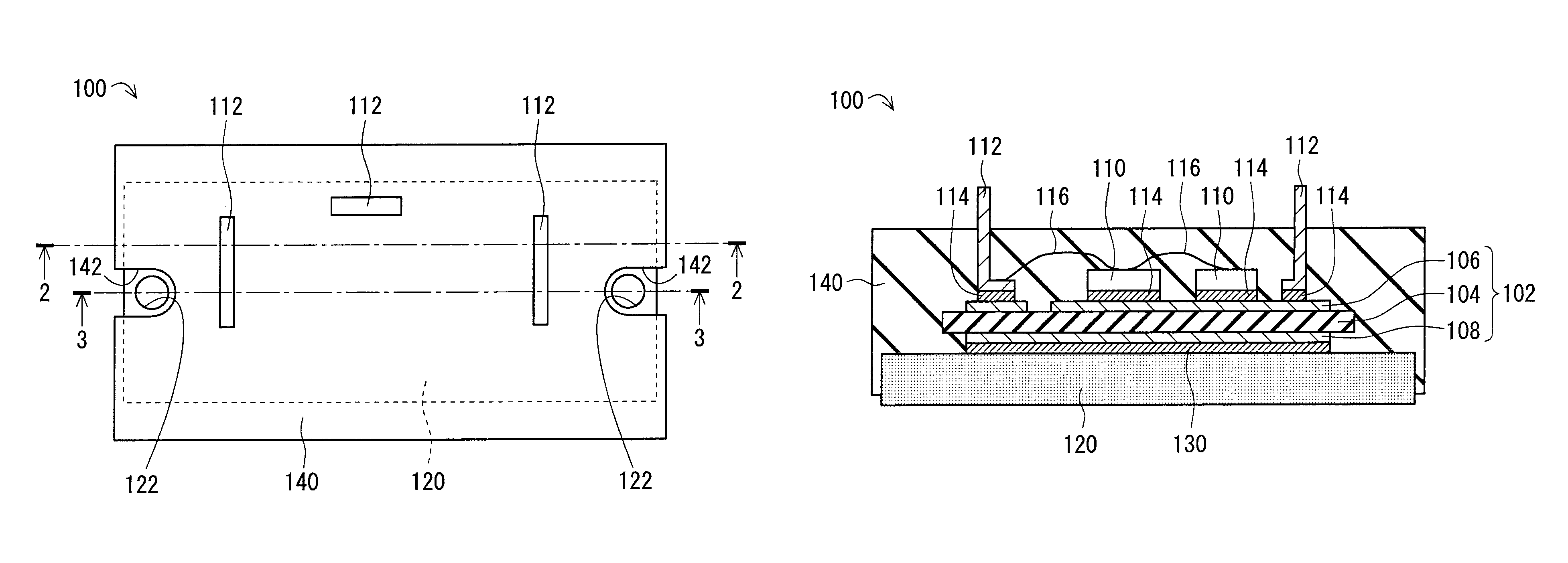
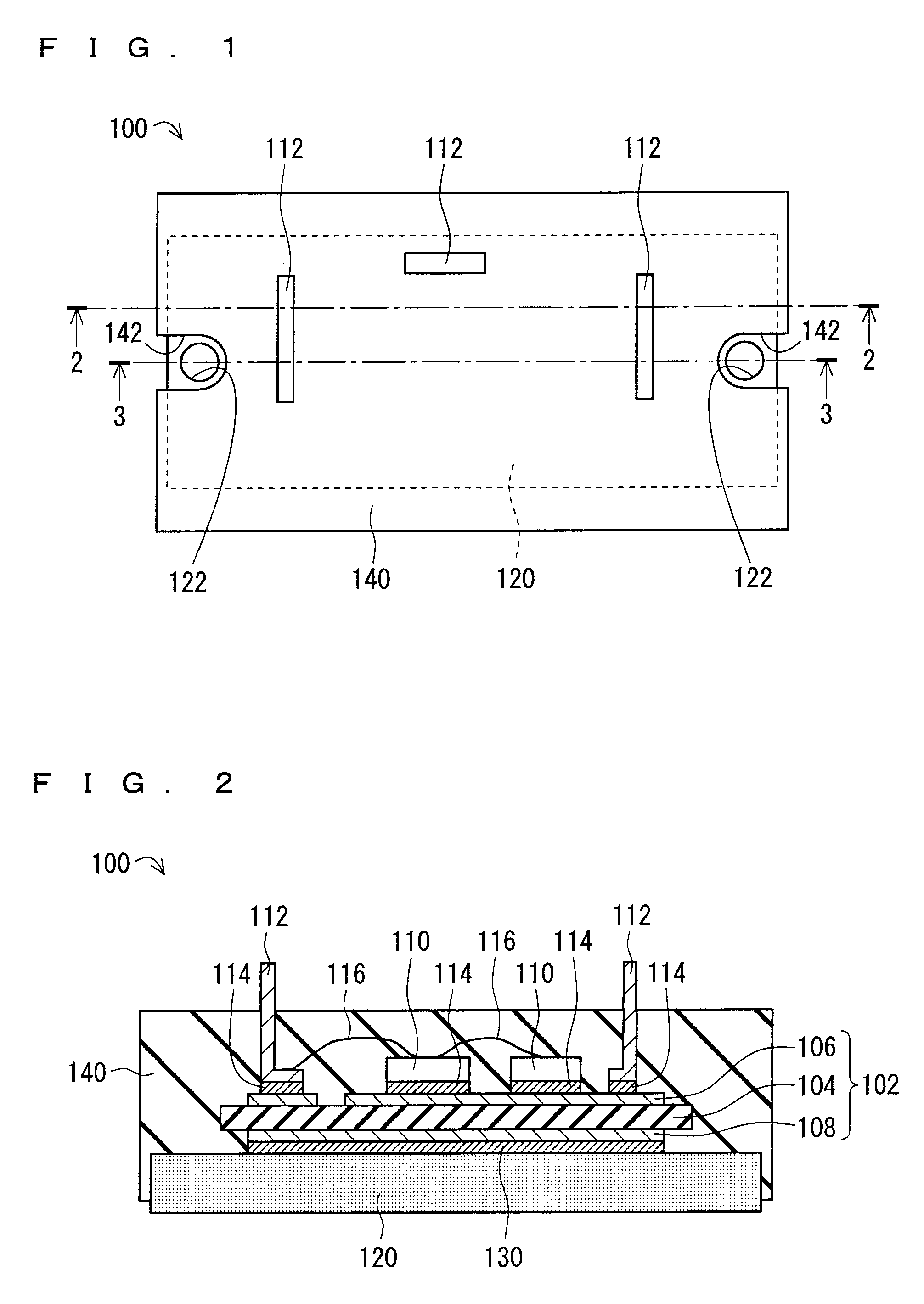
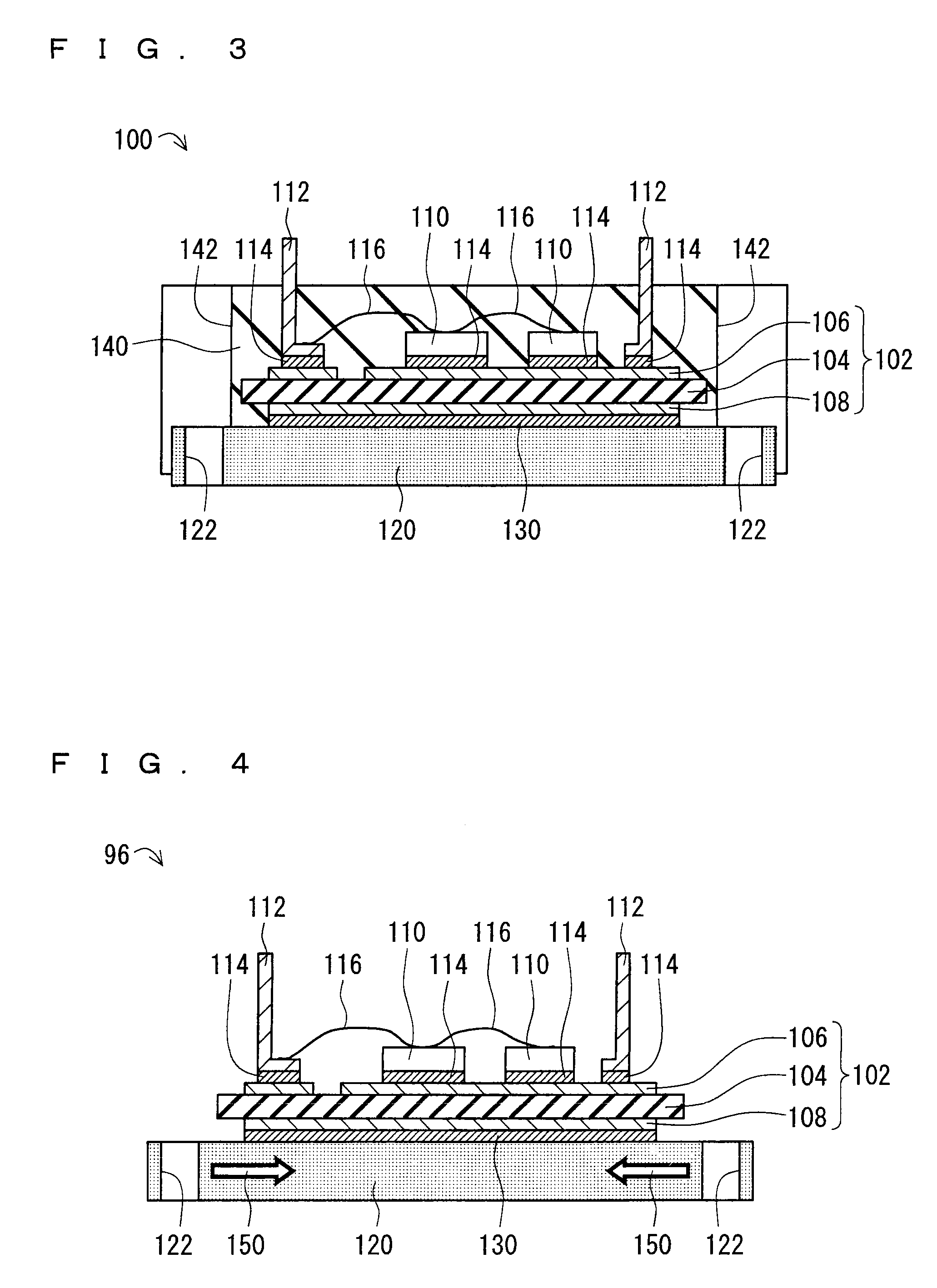
[0053]FIG. 1 shows a top view (plan view) illustrating a structure of a semiconductor device 100 in accordance with the first preferred embodiment, FIG. 2 shows a cross section taken along the line 2-2 of FIG. 1, and FIG. 3 shows a cross section taken along the line 3-3 of FIG. 1. Hereinafter, in conformity with the fact that FIG. 1 is referred to as a “top view”, the up and down direction of the semiconductor device 100 is defined. In this case, the up and down direction of FIGS. 2 and 3 corresponds to that of the semiconductor device 100. Further, hereinafter, the up and down (vertical) direction of the semiconductor device 100 is referred to as a “thickness direction”.

[0054]The semiconductor device 100 includes an insulat...


PUM


Abstract

A semiconductor device includes a base plate having one main surface joined to an insulating substrate on which a semiconductor chip and the like are mounted and a transfer mold resin which is so provided as to cover the one main surface of the base plate, the insulating substrate, the semiconductor chip, and the like and expose the other main surface of the base plate. The coefficient of linear expansion of the base plate is lower than that of copper and the coefficient of linear expansion of the transfer mold resin is not higher than 16 ppm / ° C. The transfer mold resin has such scooped shapes as to expose opposed short-side centers and the vicinity of the base plate, respectively. The base plate has mounting holes in portions exposed by the scooped shapes of the transfer mold resin.

Description

BACKGROUND OF THE INVENTION[0001]1. Field of the Invention[0002]The present invention relates to a semiconductor device, and more particularly to a structure favorable to a power semiconductor device.[0003]2. Description of the Background Art[0004]<The First Conventional Art>[0005]Case-type semiconductor devices have been conventionally known. In the case-type semiconductor device, a semiconductor chip (for example, a pair of an IGBT (Insulated Gate Bipolar Transistor) and a diode) and the like are accommodated in a package constituted of a Cu base plate and a case. More specifically, this type semiconductor device has an insulating substrate (which is formed of an insulating plate-like member (aluminum nitride, silicon nitride, alumina, or the like) with metal layers formed on both surfaces thereof), and a semiconductor chip and an electrode are soldered on the metal layer (forming a wiring pattern) formed on one surface of the insulating substrate. The metal layer formed on ...

Claims


Application Information

Patent Timeline
Patent Type & Authority Patents(United States)
IPC IPC(8): H01L23/02H01L23/31H01L23/373H01L23/433H01L25/07
CPCH01L23/3121H01L23/3735H01L23/4334H01L25/072H01L2224/45124H01L2924/00H01L2224/32225H01L2224/48137H01L2224/48227H01L2224/73265H01L2224/48091H01L2924/00014H01L2924/13055H01L2224/48139H01L2924/1305H01L2924/181H01L2924/00012
Inventor UEDA, TETSUYAYAMAGUCHI, YOSHIHIRO
Owner MITSUBISHI ELECTRIC CORP
Why Eureka
Try Eureka