
Non-volatile memory device

a memory device and non-volatile technology, applied in static storage, digital storage, instruments, etc., can solve the problems of data input to the page buffer being erroneously detected, difficult to precisely detect the state of memory cells (i.e., on-cell or off-cell) from the latch of the page buffer connected to the bit line, etc., to achieve the effect of reducing the total leakage curren

Active Publication Date: 2015-05-12
SAMSUNG ELECTRONICS CO LTD
View PDF5 Cites 5 Cited by
  • Summary
  • Abstract
  • Description
  • Claims
  • Application Information

AI Technical Summary

Benefits of technology

[0018]The present general inventive concept provides a non-volatile memory device that prevents incorrect data from being written to a latch and reduces total leakage current.
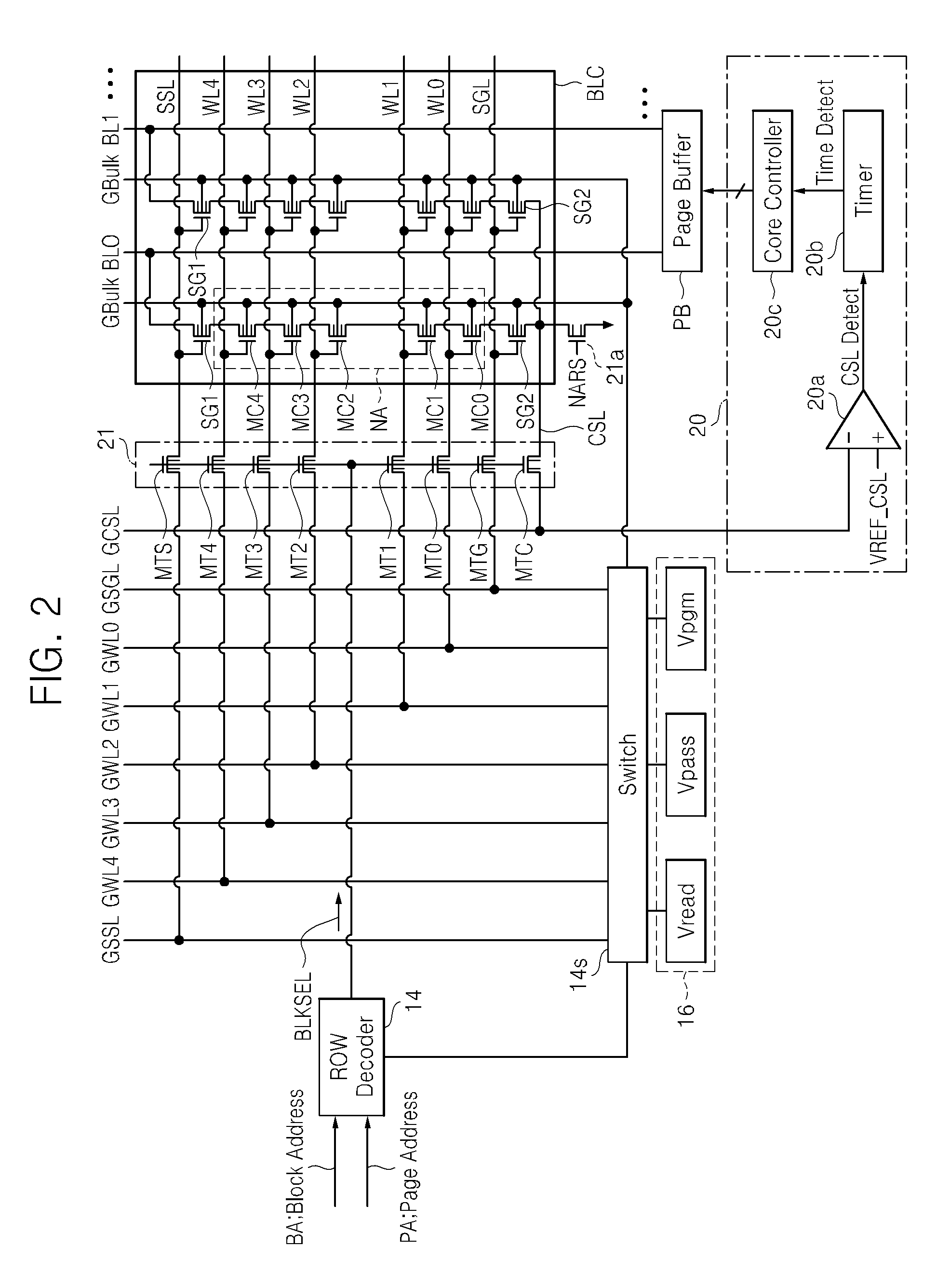
[0032]If the number of programmed memory cells greater than a predetermined threshold, a rate at which the potential of the CSL reaches the predetermined reference voltage may increase to increase a rate of data input from the one of the plurality of non-volatile memory cells to the one of the plurality of page buffers.

Problems solved by technology

As a result, the potential of a bit line does not decrease until the potential of the common source line decreases satisfactorily, and therefore, it is difficult to precisely detect a memory cell state (i.e., on-cell or off-cell) from a latch of a page buffer connected to the bit line.
However, even though the data is correctly input to the page buffer, since a latch in the page buffer detects the data, the data input to the page buffer may be erroneously detected unless the timing of the latch is controlled.

Method used


Image

  • Non-volatile memory device
  • Non-volatile memory device
  • Non-volatile memory device

Examples


Embodiment Construction

[0047]Reference will now be made in detail to the embodiments of the present general inventive concept, examples of which are illustrated in the accompanying drawings, wherein like reference numerals refer to the like elements throughout. The embodiments are described below in order to explain the present general inventive concept while referring to the figures.

[0048]It will be understood that when an element is referred to as being “connected” or “coupled” to another element, it can be directly connected or coupled to the other element or intervening elements may be present. In contrast, when an element is referred to as being “directly connected” or “directly coupled” to another element, there are no intervening elements present. As used herein, the term “and / or” includes any and all combinations of one or more of the associated listed items and may be abbreviated as “ / ”.

[0049]It will be understood that, although the terms first, second, etc. may be used herein to describe various...


PUM


Abstract

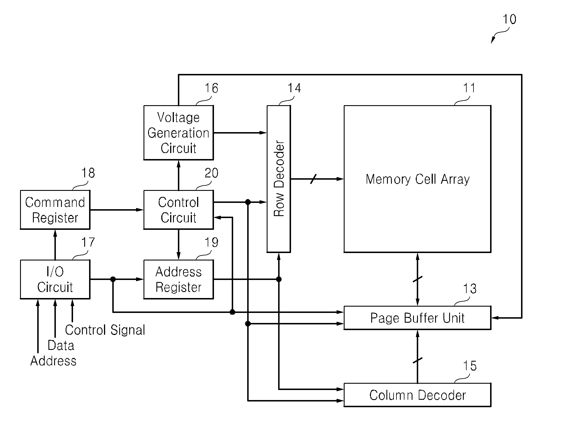
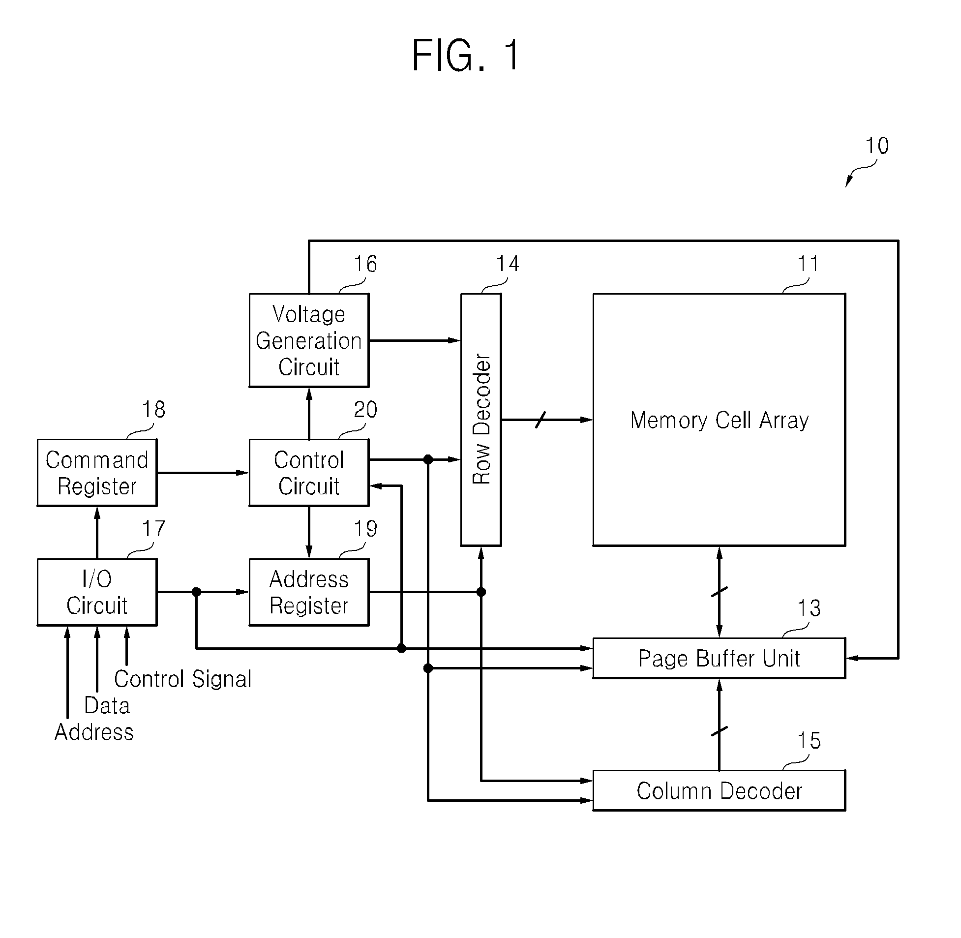
A non-volatile memory device includes a memory cell array in which a plurality of bit lines intersect a plurality of word lines and a non-volatile memory cell is disposed at each intersection, a page buffer which is provided for each bit line and which includes a latch configured to store data to be written to a memory cell connected to a word line selected from among the plurality of word lines or data read from the memory cell, and a control circuit configured to control a data input time from the bit line to the page buffer and a data detection time of the latch according to a voltage level of a common source line connected to sources of the respective bit lines during an operation of reading data from the memory cell.

Description

CROSS-REFERENCE TO RELATED APPLICATIONS[0001]This application claims priority under 35 U.S.C. §119(a) from Japanese Patent Application No. 2011-275702 filed on Dec. 16, 2011, the disclosure of which is hereby incorporated by reference in its entirety.BACKGROUND[0002]1. Field[0003]Embodiments of the present general inventive concept relate to a non-volatile memory device.[0004]2. Description of the Related Art[0005]When a read operation is performed in a non-volatile memory device, e.g., electrically erasable programmable read-only memory (EEPROM), with a large capacity, data is read in bulk from a plurality of memory cells in a page at one time and output in series. When a write operation is performed on memory cells, data of a page is input in series to the non-volatile memory device and it is written in bulk to a plurality of memory cells at one time. To perform the read or write operation, a plurality of columns, i.e., bit lines are connected to a page buffer including a data lat...

Claims


Application Information

Patent Timeline
Patent Type & Authority Patents(United States)
IPC IPC(8): G11C16/04G11C16/06G11C16/08G11C16/26G11C16/32G11C16/34
CPCG11C16/06G11C16/08G11C16/26G11C16/32G11C16/3436G11C16/0483
Inventor MIYAMOTO, TOMOHISA
Owner SAMSUNG ELECTRONICS CO LTD
Learn More