Plasma processing apparatus, plasma processing method and storage medium for storing program for executing the method

a technology of plasma processing and program execution, which is applied in the direction of plasma technique, coating, electric discharge lamps, etc., can solve the problems of non-uniform voltage applied to the periphery of the substrate, affecting and reducing the top surface electric potential of the focus ring to a level lower than the desired potential, etc., to achieve the effect of increasing the processing rate of the deposit etching process and reducing the top surface electric potential

Active Publication Date: 2015-07-07
TOKYO ELECTRON LTD
View PDF10 Cites 19 Cited by
  • Summary
  • Abstract
  • Description
  • Claims
  • Application Information

AI Technical Summary

Benefits of technology

[0014]In accordance with the present disclosure, the dielectric constant of the dielectric ring may be adjusted by the dielectric constant varying device without exchanging the dielectric ring even when the type of the substrate is changed. Accordingly, a current may easily flow from the susceptor toward the focus ring, whereas a current may hardly flow from the substrate toward the focus ring. As a result, it is possible to apply the uniformized voltage to the periphery of the substrate and suppress the decrease in the top surface electric potential of the focus ring.
[0015]Further, since the top surface electric potential of the focus ring is not changed depending on the type of the substrate, the top surface electric potential of the focus ring may be maintained at a high level by adjusting the dielectric constant of the dielectric ring. Accordingly, it is possible to improve a processing rate of the process at the periphery of the substrate or the deposit etching process.
[0020]In accordance with the present disclosure, without exchanging the dielectric ring even when the type of the substrate is changed, the dielectric constant of the dielectric ring may be adjusted by vertically moving the conductor in the space within the dielectric ring. Accordingly, a current may easily flow from the susceptor toward the focus ring, whereas a current may hardly from the substrate toward the focus ring. As a result, it may be possible to apply the uniformized voltage to the periphery of the substrate and suppress the decrease in the top surface electric potential of the focus ring.
[0022]With this configuration, by vertically moving the grounding body, the top surface electric potential of the focus ring may be adjusted while maintaining the dielectric constant of the dielectric ring. Further, during the deposit etching process at the substrate periphery, the top surface electric potential of the focus ring may be reduced by adjusting the position of the grounding body toward the focus ring. Accordingly, a large potential difference between the substrate (susceptor) and the inner periphery of the focus ring may be generated. As a result, it may be possible to increase the processing rate of the deposit etching process while maintaining the dielectric constant of the dielectric ring.
[0023]In accordance with the present disclosure, there is provided the dielectric constant varying device capable of adjusting the dielectric constant of the dielectric ring provided between the focus ring and the susceptor. Accordingly, the dielectric constant of the dielectric ring may be adjusted without exchanging the dielectric ring. As a result, it may be possible to apply the uniformized voltage to the periphery of the substrate, and also possible to control the top surface electric potential of the focus ring to a desired value.

Problems solved by technology

Accordingly, there are problems that a voltage applied to the periphery of the substrate may become non-uniform, and the top surface electric potential of the focus ring may be decreased to a level lower than a desired potential.
As a result, the top surface electric potential of the focus ring may become non-uniform depending on a type of substrate.

Method used


Image

  • Plasma processing apparatus, plasma processing method and storage medium for storing program for executing the method
  • Plasma processing apparatus, plasma processing method and storage medium for storing program for executing the method
  • Plasma processing apparatus, plasma processing method and storage medium for storing program for executing the method

Examples


Embodiment Construction

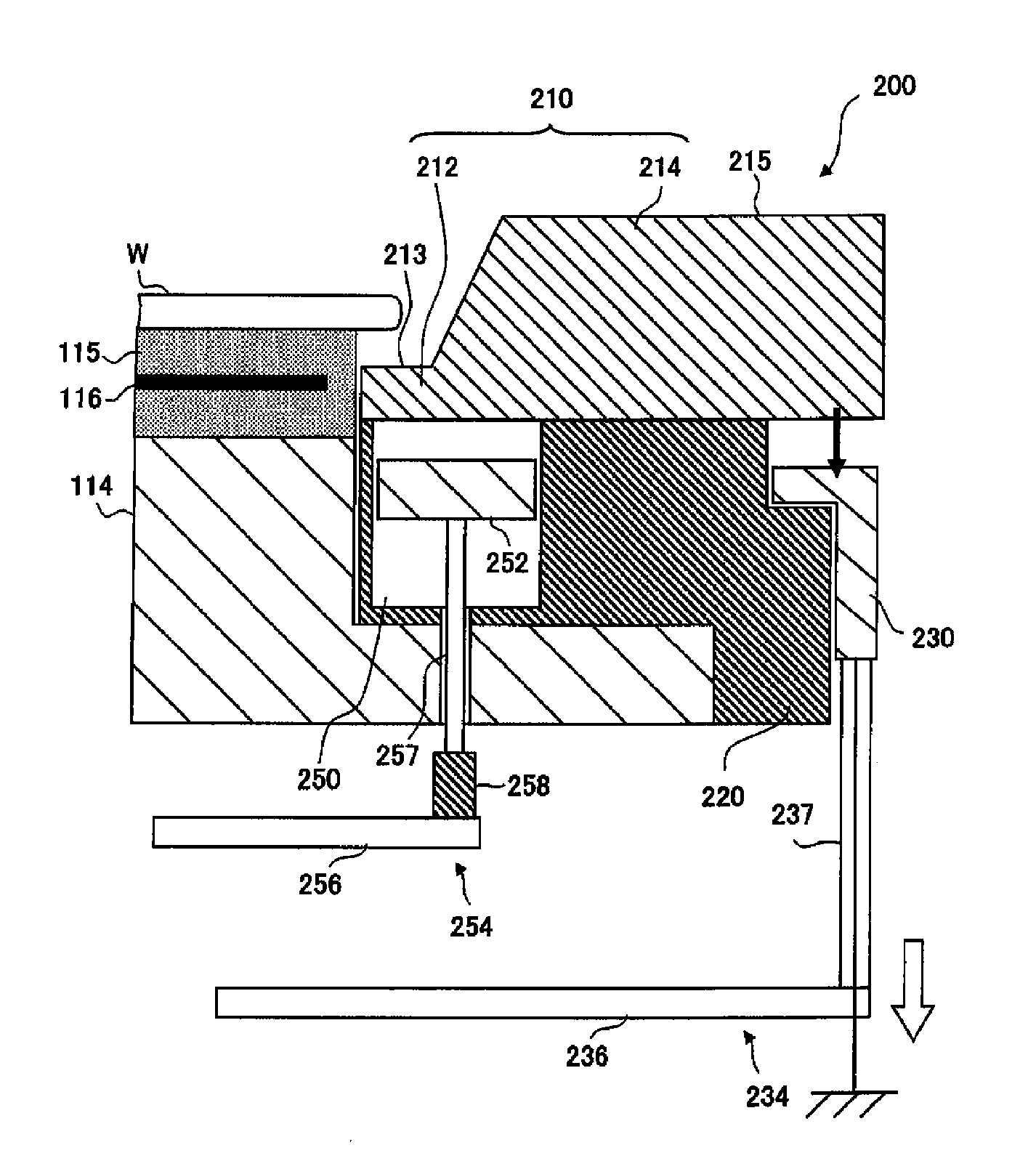
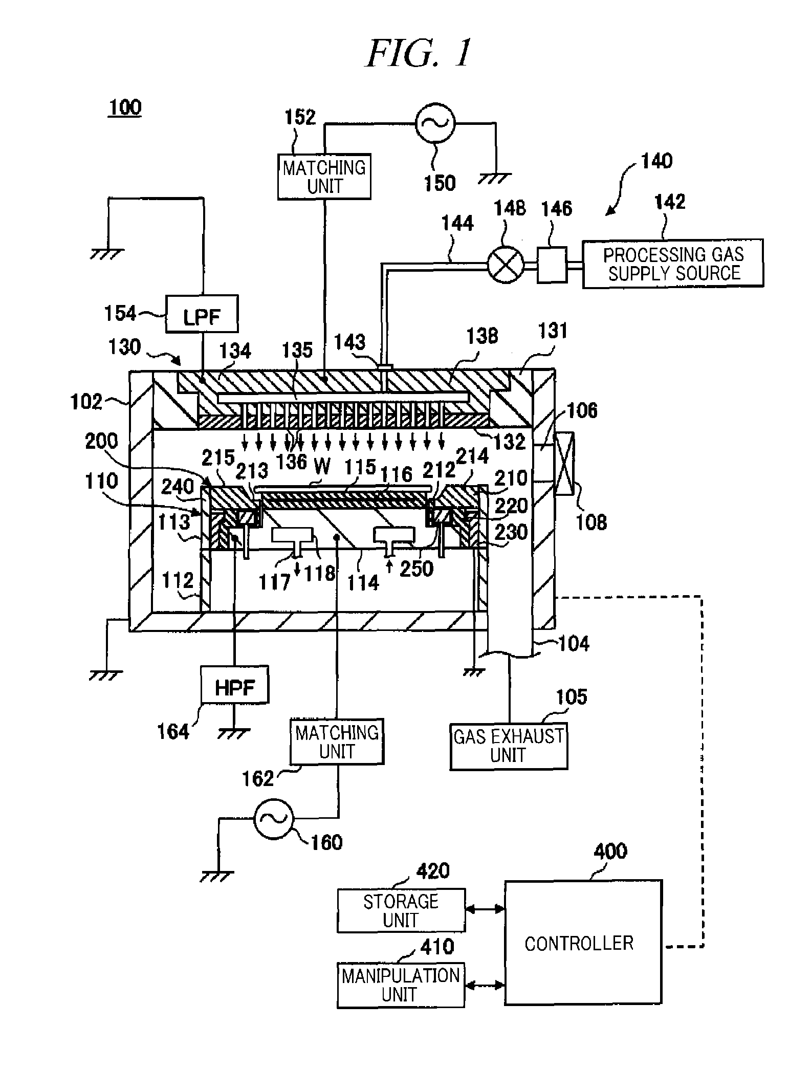
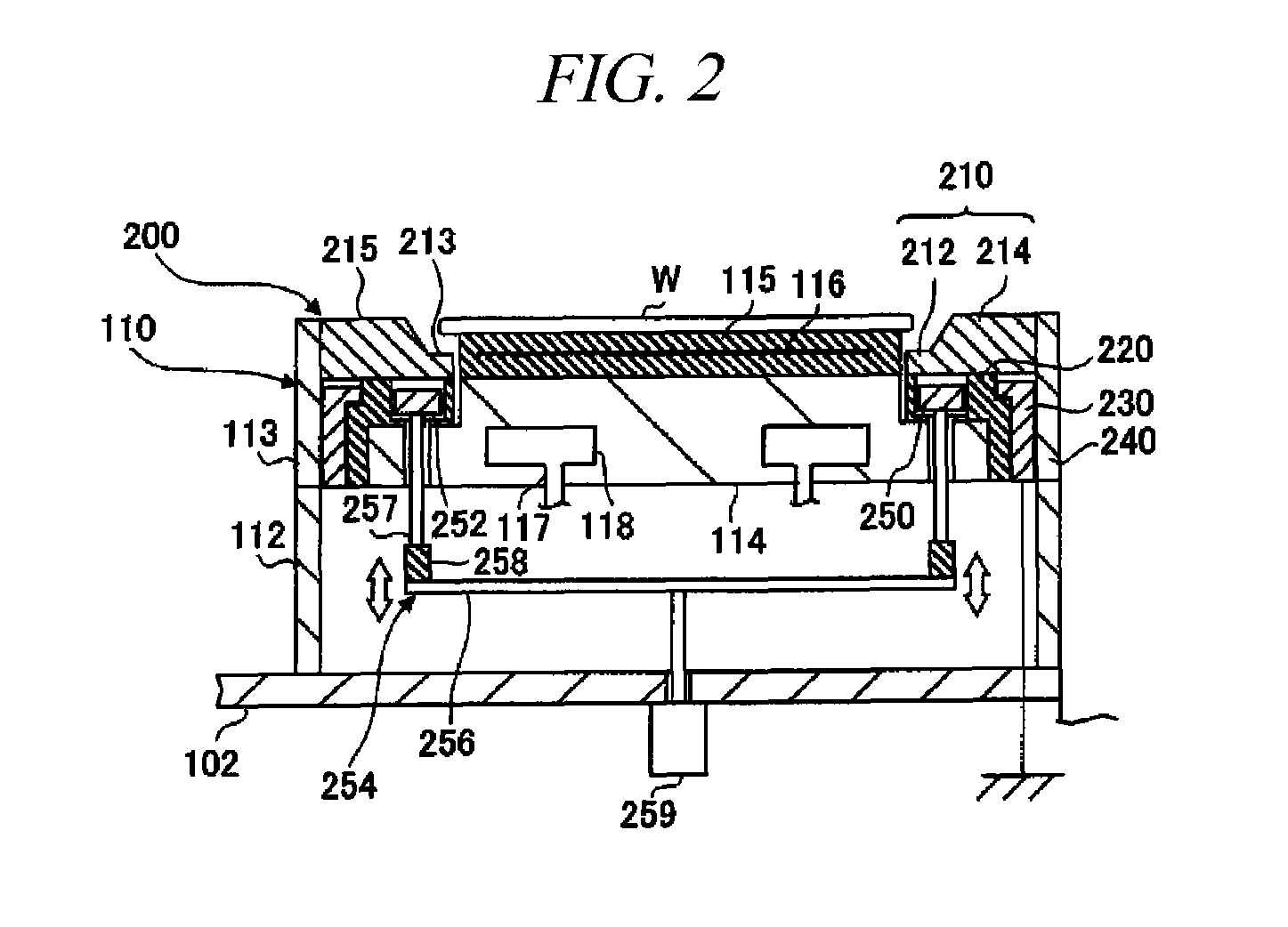
[0042]Hereinafter, the embodiments of the present disclosure will be described in detail with reference to the accompanying drawings. In the specification and the accompanying drawings, same reference numerals will be given to same parts having substantially the same functions and configurations, and redundant description thereof will be omitted.

[0043](Configuration Example of Plasma Processing Apparatus)

[0044]First, a schematic configuration of a plasma processing apparatus in accordance with an embodiment of the present disclosure will be described with reference to the accompanying drawings. Here, a parallel plate type plasma processing apparatus will be explained as an example apparatus. FIG. 1 is a longitudinal cross sectional view showing a schematic configuration of a plasma processing apparatus 100 in accordance with the embodiment of the present disclosure.

[0045]The plasma processing apparatus 100 may include a processing chamber 102 having therein a cylindrical processing ...


PUM

PropertyMeasurementUnit
DC voltageaaaaaaaaaa
frequencyaaaaaaaaaa
frequencyaaaaaaaaaa

Abstract

There is provided a plasma processing apparatus including a susceptor 114, having a substrate mounting portion for mounting thereon a substrate, to which a high frequency power is applied; a focus ring 210, disposed to surround the substrate mounted on the substrate mounting portion, including an outer ring 214 having a top surface higher than a top surface of the substrate and an inner ring 212 extending inwardly from the outer ring so as to allow at least a part of the inner ring to be positioned below a periphery of the substrate, the outer ring and the inner ring being formed as a single member; a dielectric ring 220 positioned between the focus ring and the susceptor; a dielectric constant varying device 250 for varying a dielectric constant of the dielectric ring.

Description

CROSS-REFERENCE TO RELATED APPLICATION[0001]This application claims the benefit of Japanese Patent Application No. 2010-206020 filed on Sep. 14, 2010 and U.S. Provisional Application Ser. No. 61 / 389,425 filed on Oct. 4, 2010, the entire disclosures of which are incorporated herein by reference.FIELD OF THE INVENTION[0002]The present disclosure relates to a plasma processing apparatus including a focus ring disposed to surround a periphery of a substrate, and also relates a plasma processing method and a storage medium for storing a program for executing the plasma processing method.BACKGROUND OF THE INVENTION[0003]In manufacturing processes of a semiconductor device, in order to form a micro circuit pattern on a substrate such as a semiconductor wafer, a FPD substrate or a substrate for a solar cell, a certain process such as an etching process or a film formation process is repetitively performed on the substrate. Such process is carried out by a plasma processing apparatus.[0004]T...

Claims


Application Information

Patent Timeline
Patent Type & Authority Patents(United States)
IPC IPC(8): C23C16/00H01L21/306H01L21/687H01L21/67H01J37/32H05B31/26H01J7/24C23F1/00
CPCH01J37/32642H01J37/32091H01L21/67069H01L21/68735C23C16/52
Inventor OHATA, MITSUNORIKIMURA, HIDETOSHIMAEDA, KIYOSHIHIROSE, JUNHIDA, TSUYOSHI
Owner TOKYO ELECTRON LTD
Why Eureka
Try Eureka