Nanostructured thermolectric elements and methods of making the same

a technology of thermoelectric elements and nanostructures, applied in the field of nanostructured thermoelectric elements and methods of making the same, can solve the problems of limited commercial application of thermoelectric devices, poor cost performance of these devices, and the limited range of thermoelectric devices, and achieve the effect of reducing the cost of thermoelectric devices and reducing the cost of production

Inactive Publication Date: 2015-07-14
SYNERGY THERMOGEN INC +1
View PDF135 Cites 14 Cited by
  • Summary
  • Abstract
  • Description
  • Claims
  • Application Information

AI Technical Summary

Problems solved by technology

To date, thermoelectrics have had limited commercial applicability due to the poor cost performance of these devices compared to other technologies that accomplish similar means of energy generation or refrigeration.
Where other technologies usually are not as suitable as thermoelectrics for using in lightweight and low footprint applications, thermoelectric devices often have nonetheless been limited by their prohibitively high costs.
The thermoelectric materials in presently available commercial thermoelectric modules are generally comprised of bismuth telluride or lead telluride, which are both toxic, difficult to manufacture with, and expensive to procure and process.
However, many drawbacks may exist in the production of conventional thermoelectric devices.
For ...

Method used


Image

  • Nanostructured thermolectric elements and methods of making the same
  • Nanostructured thermolectric elements and methods of making the same
  • Nanostructured thermolectric elements and methods of making the same

Examples


Embodiment Construction

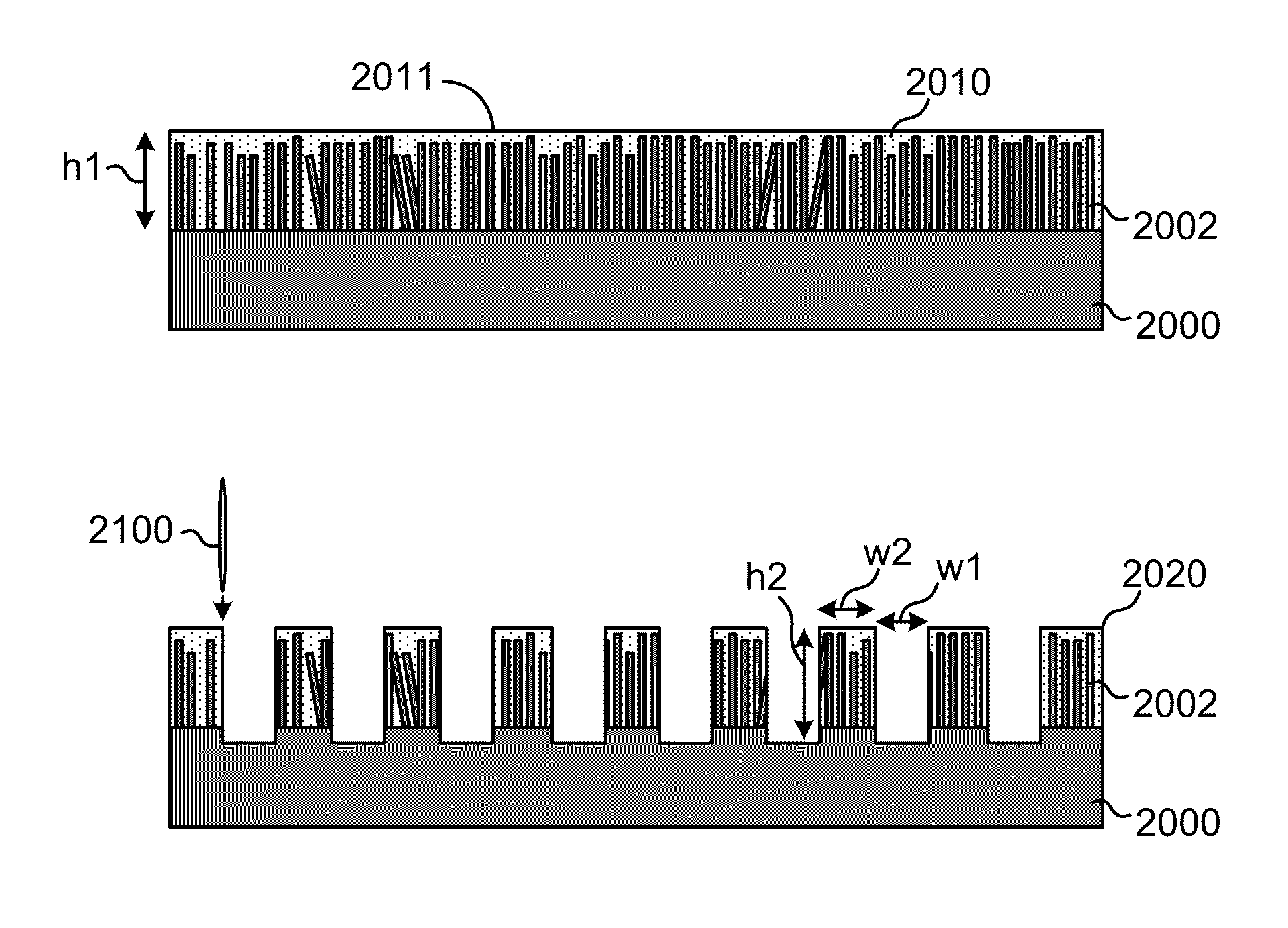
[0023]The present invention is directed to thermoelectric structure and method of making the same. More particularly, the invention provides a method for the manufacture of nanostructured thermoelectric elements. Merely by way of an example, the method has been applied to uniwafer backend processing for forming a plurality of thermoelectric legs based on nanowires in a single silicon wafer. It would be recognized that the invention has a much broader range of applicability.

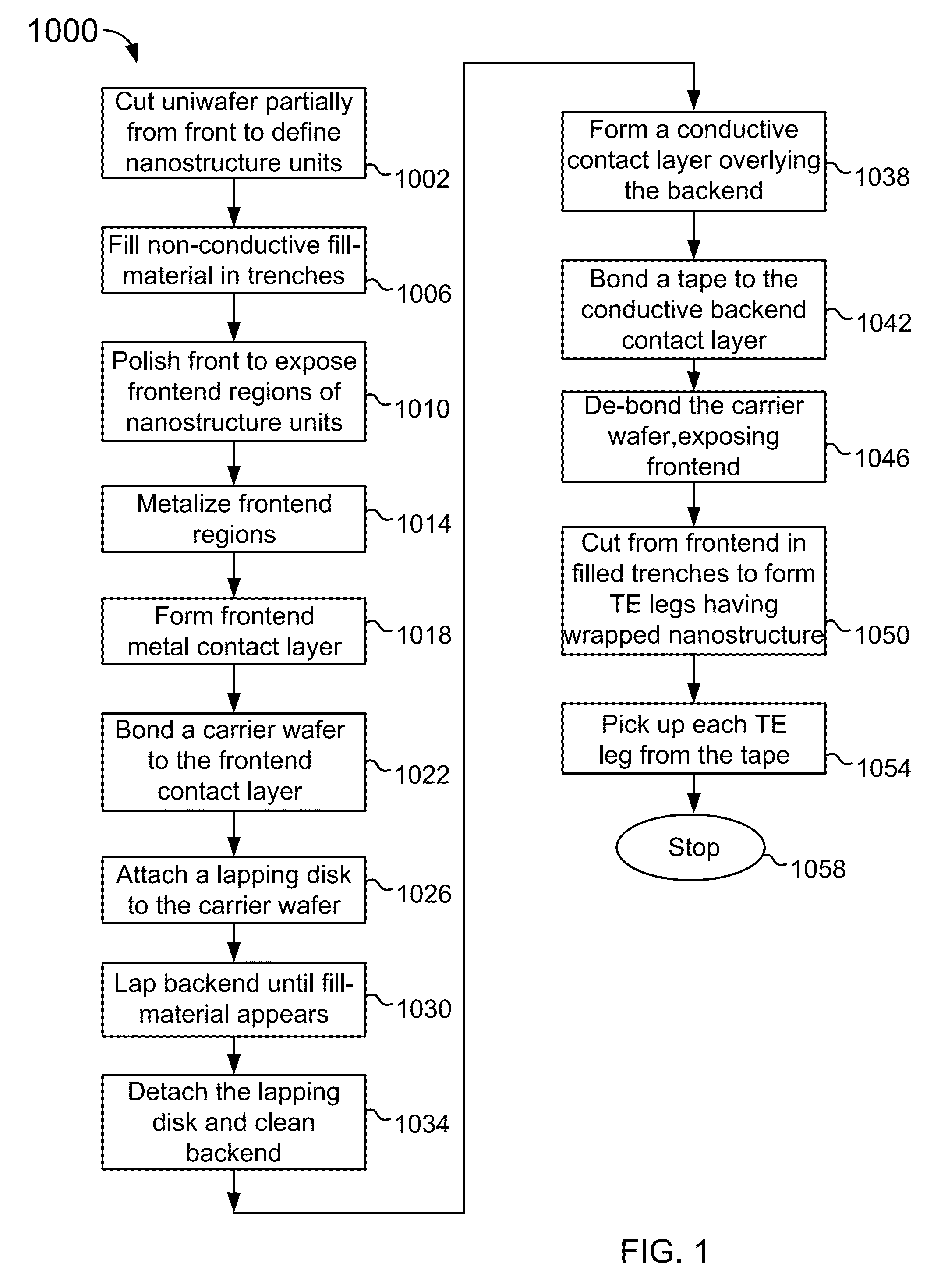
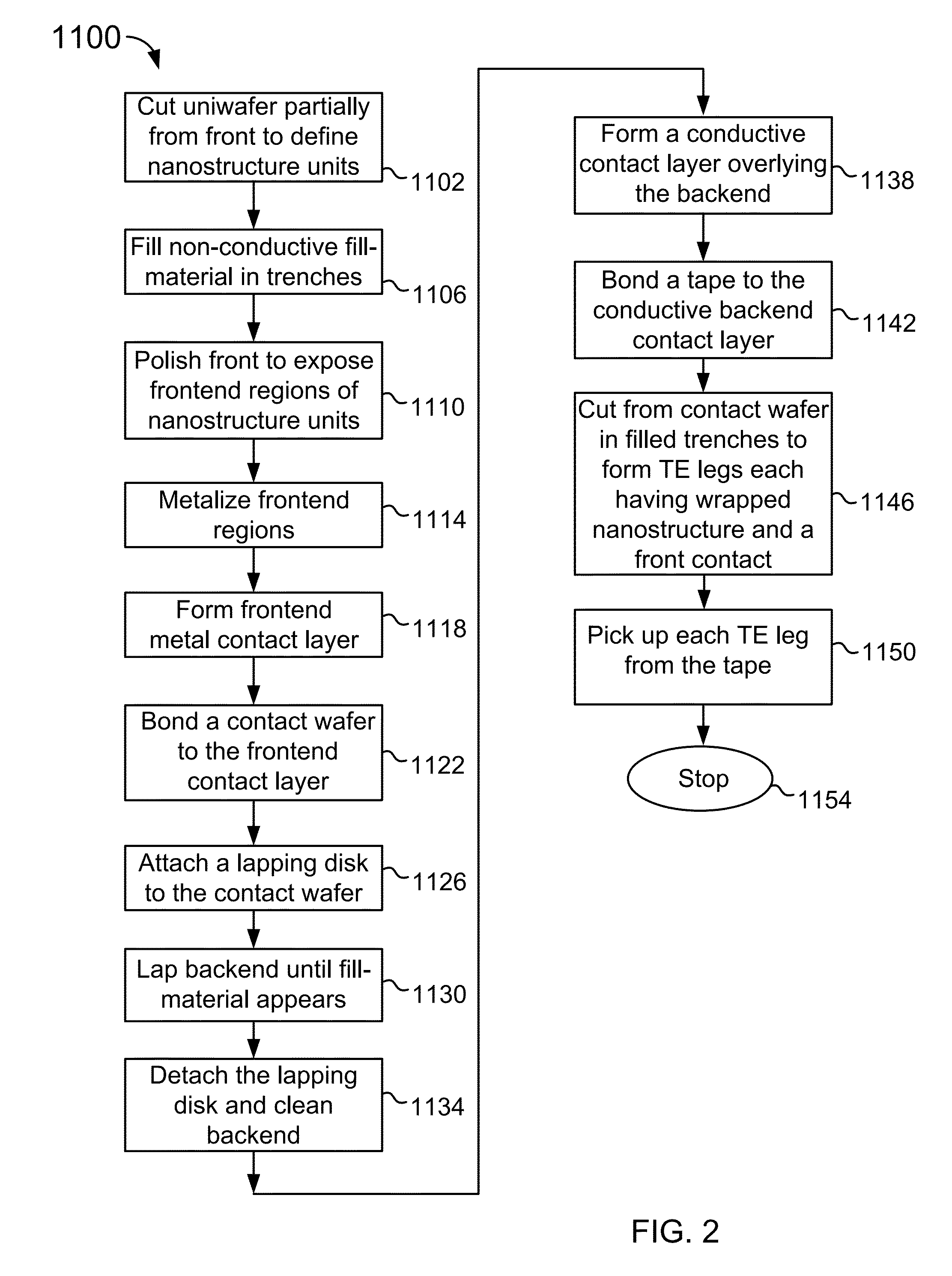
[0024]After the formation of the various type nanostructure arrays, including nanowires, nanotubes, nanoholes, or a mesh network of above nanostructures, filled with a matrix of low-thermal conductivity fill material embedded in a silicon wafer, the overall structure remains a single wafer. Thus, planar silicon wafer processing technology may be borrowed in certain aspects to manufacture a plurality of bulk-sized thermoelectric legs out of this uniwafer structure. Several methods are introduced in terms of flow ch...


PUM


Abstract

Nanostructured thermoelectric elements are made from planar uniwafer processing methods. The method includes producing either n-type or p-type thermoelectric uniwafer structure bearing nanostructure material embedded in a low thermal conductivity fill material. The method further includes partially cutting the uniwafer structure to form a plurality of chip structures separated by trenches. The method includes filling the trenches with the fill material to surround the nanostructure material within each chip structure. The method further includes additionally planar processing to form both frontend and backend conductive contact layers respectively coupled to frontend regions and backend regions of the chip structures. Additionally, the modified thermoelectric uniwafer structure is cut to turn the chip structures to bulk-sized nanostructured thermoelectric legs, each bulk-sized nanostructured thermoelectric leg being wrapped around by the fill material and ready for assembling thermoelectric modules.

Description

CROSS-REFERENCES TO RELATED APPLICATIONS[0001]This application claims priority of U.S. Provisional Patent Application No. 61 / 718,572, filed on Oct. 25, 2012, commonly assigned, and hereby incorporated by reference in its entirety herein for all purposes.[0002]This application is also related to U.S. patent application Ser. Nos. 13 / 299,179, 13 / 308,945, and 13 / 331,768, commonly assigned, and hereby incorporated by references in their entireties herein for all purposes.BACKGROUND OF THE INVENTION[0003]The present invention is directed to thermoelectric structure and method of making the same. More particularly, the invention provides a method for the manufacture of nanostructured thermoelectric elements. Merely by way of an example, the method has been applied to uniwafer backend processing for forming a plurality of thermoelectric legs based on nanowires in a single silicon wafer. It would be recognized that the invention has a much broader range of applicability.[0004]To date, thermo...

Claims


Application Information

Patent Timeline
IPC IPC(8): H01L21/00H01L35/34
CPCH01L35/34H10N10/01H10N10/17
Inventor WACKER, BARBARAAGUIRRE, MARIO
Owner SYNERGY THERMOGEN INC
Why Eureka
Try Eureka