

Method and system for recycling processing gas for selenization of thin film photovoltaic materials
a technology of photovoltaic materials and processing gas, which is applied in the direction of selenium/tellurium compounds with other elements, dispersed particle separation, and separation processes, etc. it can solve the problems of insufficient in various situations, the relative cost of selenide species as a work gas not only affects the quality of the material, but also the potential environmental hazards, etc., to achieve cost saving, reduce the waste of valuable work material, and reduce the effect of was
- Summary
- Abstract
- Description
- Claims
- Application Information
AI Technical Summary
Benefits of technology
Problems solved by technology
Method used
Image

Examples
Embodiment Construction
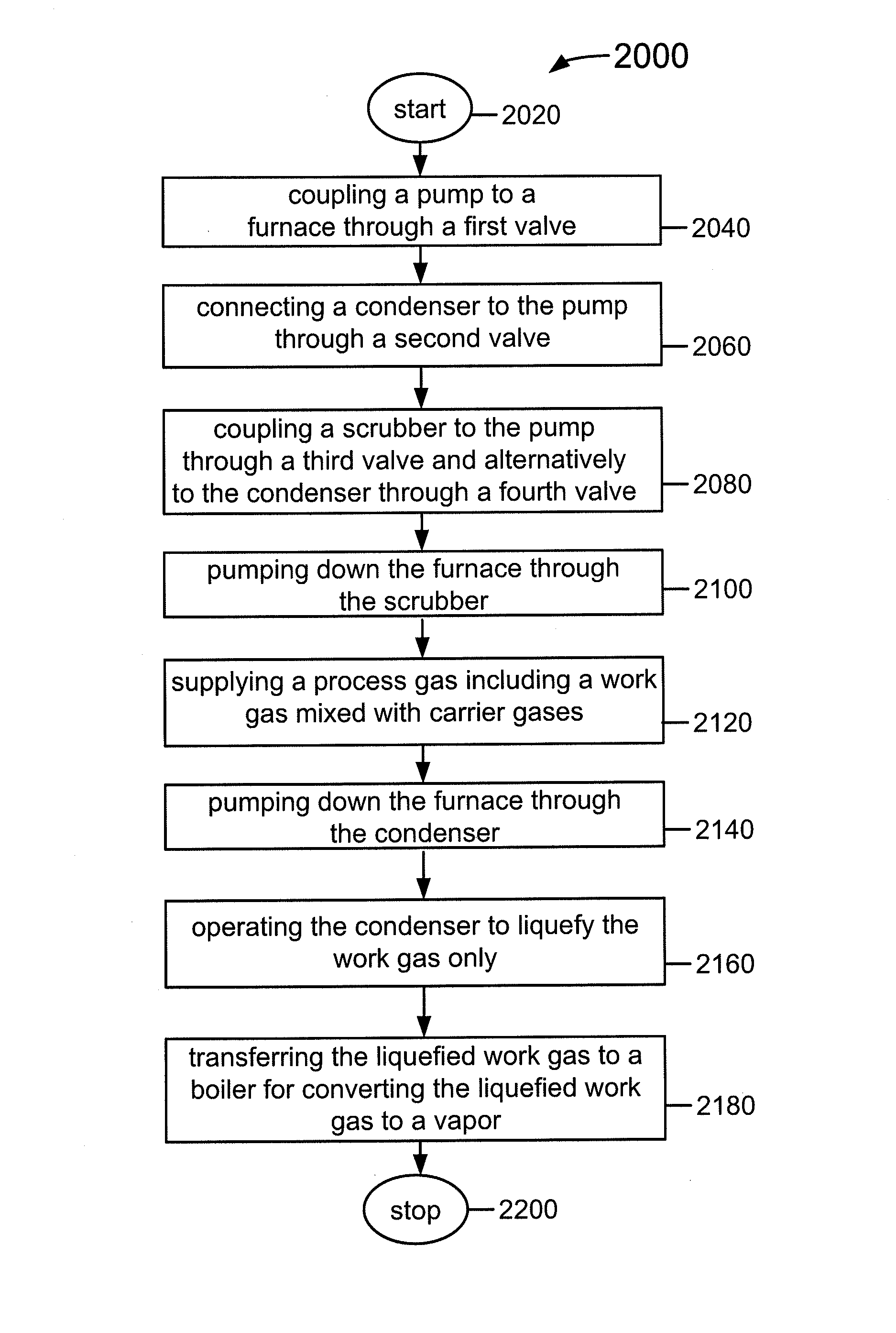
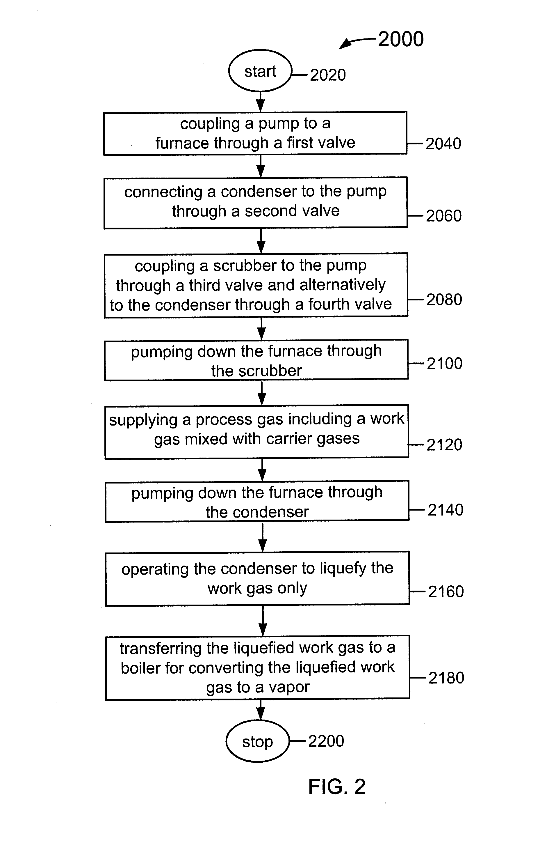
[0010]The present invention relates generally to thin-film photovoltaic techniques. More particularly, the present invention provides a system and method for handling work gas used for the manufacture of thin-film photovoltaic devices based on copper indium diselenide species (CIS), copper indium gallium diselenide species (CIGS), and / or others. The invention can be applied to made CIGS photovoltaic modules on panels, flexible sheets, building or window glass, automotive, and others.
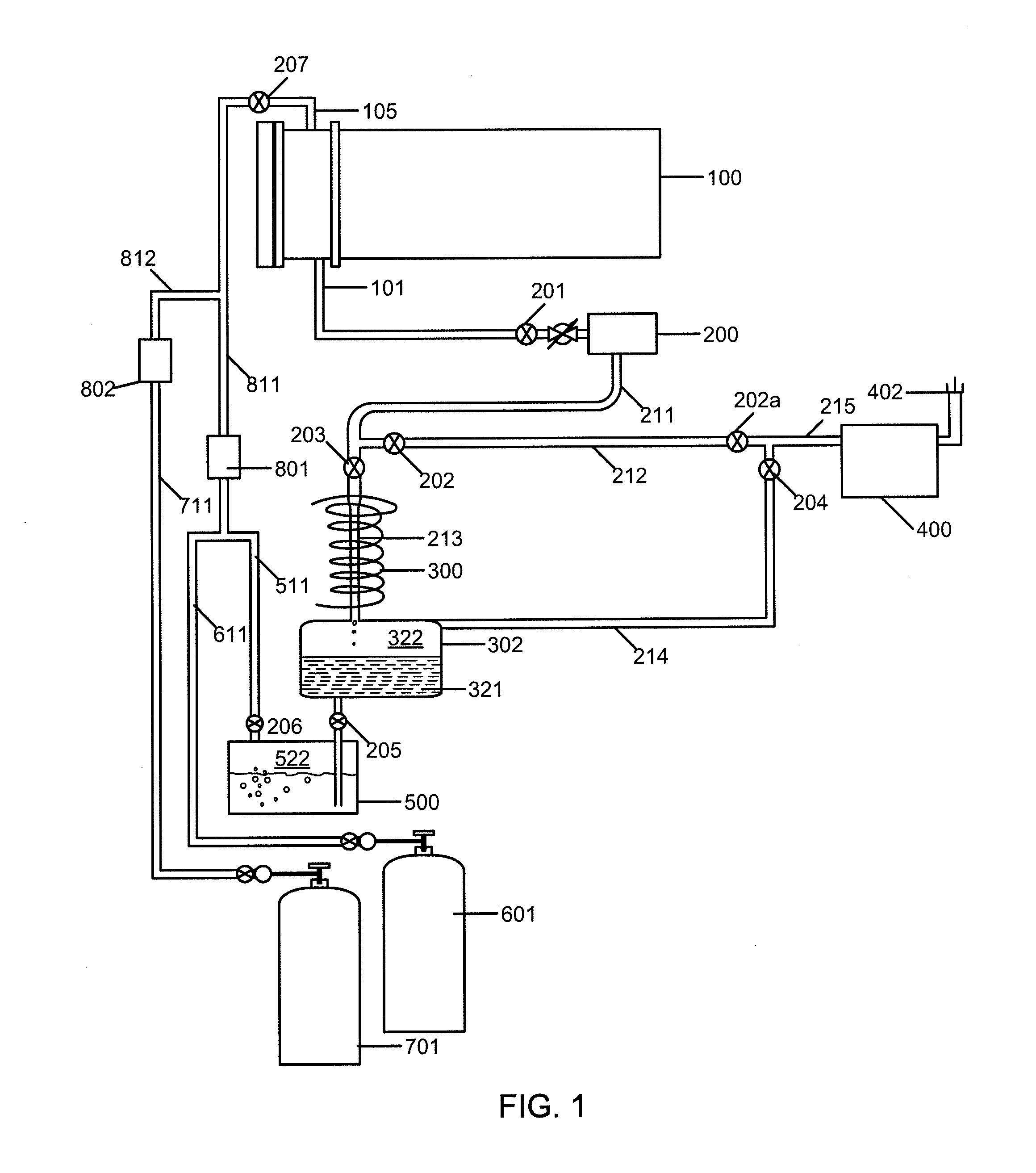
[0011]FIG. 1 is a diagram of a system for recycling a work gas for the manufacture of CIGS photovoltaic device according to an embodiment of the present invention. As shown, the system 1000 is associated with a process furnace or thermal reactor 100 that is configured to perform thermal reactive treatment of thin-film devices under a gaseous environment within the furnace. In an example, the thermal reactor 100 is applied to treat thin-film photovoltaic devices using a process gas 101 comprising a mixtur...
PUM
| Property | Measurement | Unit |
|---|---|---|
| total pressure | aaaaa | aaaaa |
| pressure | aaaaa | aaaaa |
| boiling point | aaaaa | aaaaa |
Abstract
Description
Claims
Application Information