Array substrate and method for manufacturing the same, display apparatus

a technology of array substrate and array substrate, which is applied in the field of array substrate, can solve the problems of poor resistance uniformity in the direction perpendicular to the gate signal line, high resistance of the common electrode of the ffs mode of liquid crystal display panel, and the inability to uniformly distribute the voltage on the common electrode, so as to improve the image display quality of the display apparatus, reduce the resistance, and improve the effect of resistance uniformity

Active Publication Date: 2015-09-01
BOE TECH GRP CO LTD +1
View PDF2 Cites 3 Cited by
  • Summary
  • Abstract
  • Description
  • Claims
  • Application Information

AI Technical Summary

Benefits of technology

[0009]According to an object of the present invention, there is provided an array substrate, a method for manufacturing the array substrate, and a display apparatus comprising the array substrate, in which a common electrode of the array substrate has reduced resistance and improved resistance uniformity in a direction perpendicular to a gate signal line, thereby improving the image display quality of the display apparatus.

Problems solved by technology

In sum, in the prior art, the common electrode of the FFS mode of liquid crystal display panel has high resistance and poor resistance uniformity in the direction perpendicular to the gate signal line.
As a result, voltage cannot be uniformly distributed on the common electrode, and it likely leads to various defects, for example, residual image, occurring in the liquid crystal display panel.

Method used


Image

  • Array substrate and method for manufacturing the same, display apparatus
  • Array substrate and method for manufacturing the same, display apparatus
  • Array substrate and method for manufacturing the same, display apparatus

Examples


Embodiment Construction

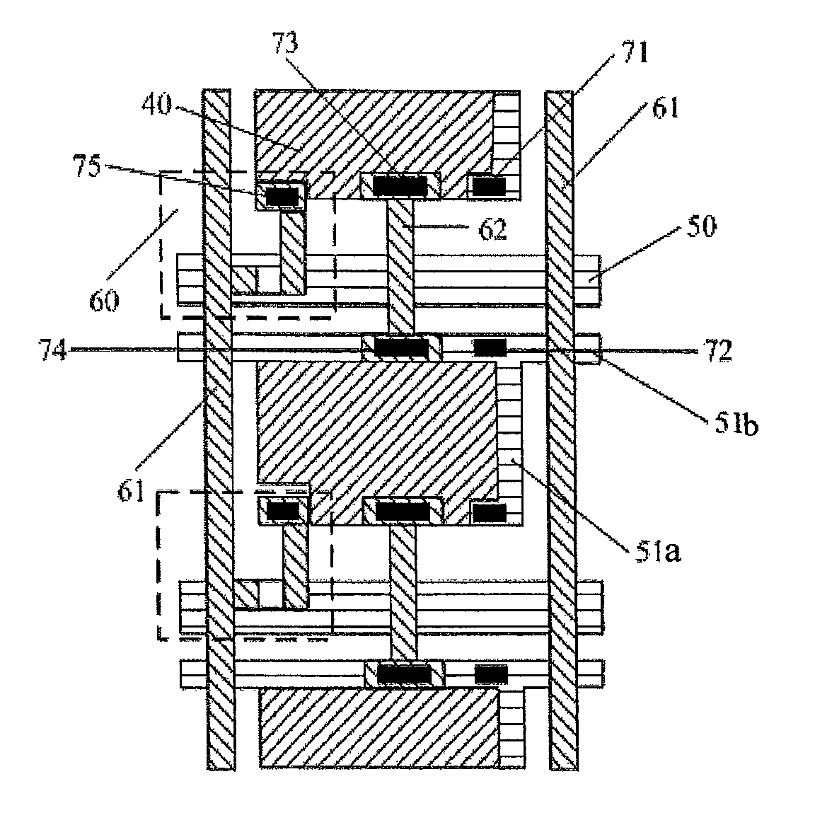
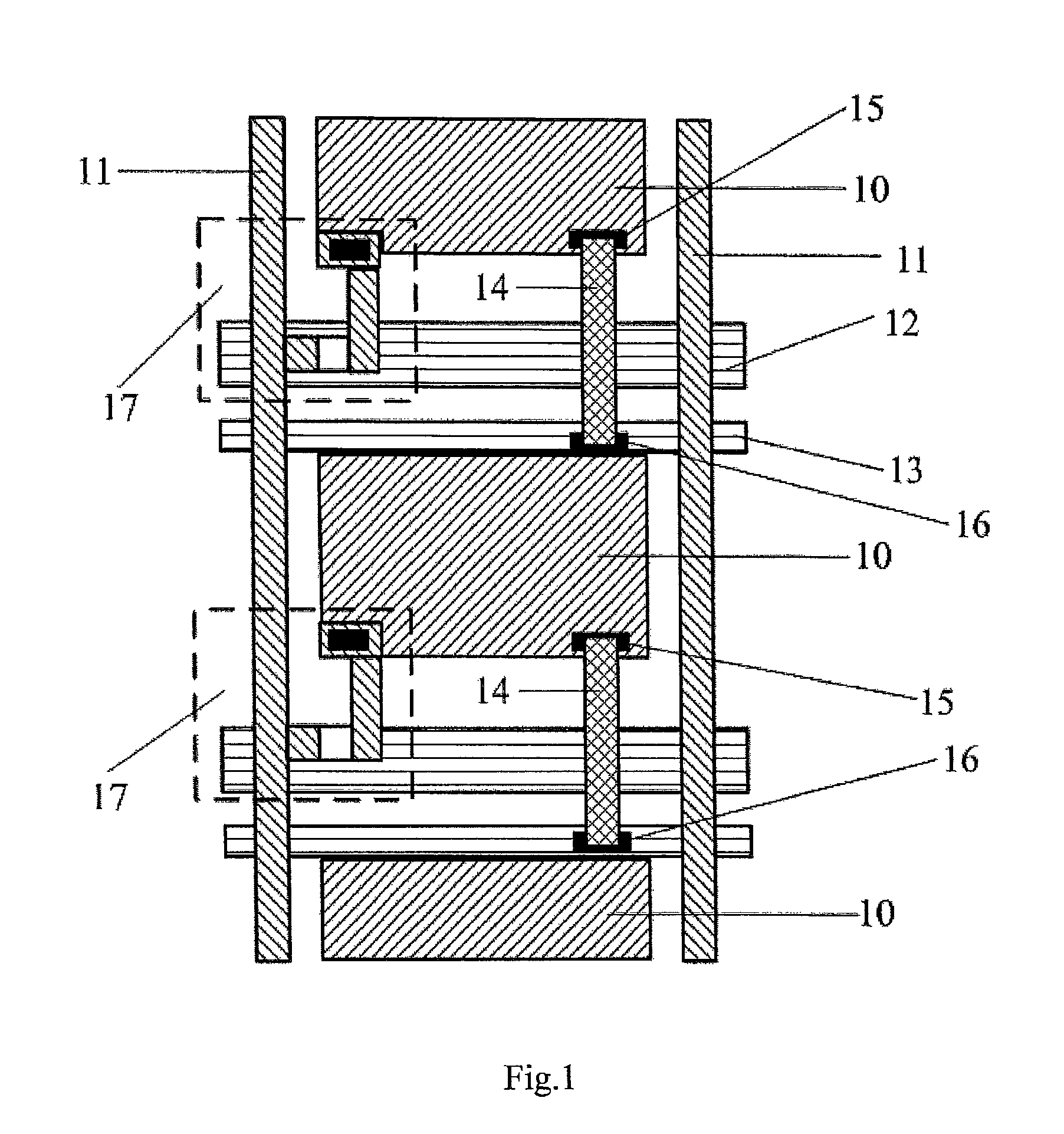
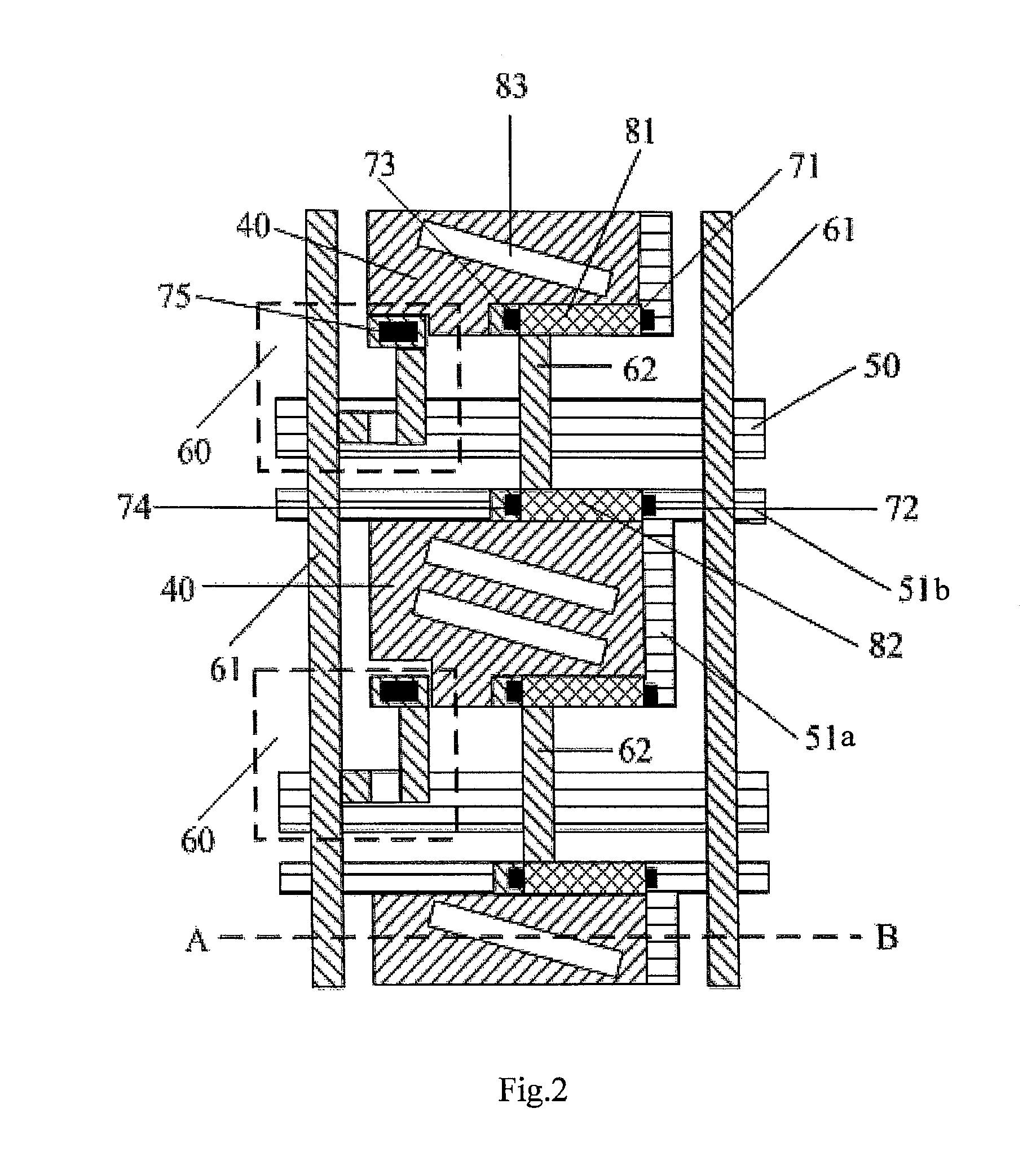
[0034]Exemplary embodiments of the present disclosure will be described hereinafter in detail with reference to the attached drawings, wherein the like reference numerals refer to the like elements. The present disclosure may, however, be embodied in many different forms and should not be construed as being limited to the embodiment set forth herein; rather, these embodiments are provided so that the present disclosure will be thorough and complete, and will fully convey the concept of the disclosure to those skilled in the art.

[0035]In the following detailed description, for purposes of explanation, numerous specific details are set forth in order to provide a thorough understanding of the disclosed embodiments. It will be apparent, however, that one or more embodiments may be practiced without these specific details. In other instances, well-known structures and devices are schematically shown in order to simplify the drawing.

[0036]According to a general concept of the present inv...


PUM

PropertyMeasurementUnit
electricallyaaaaaaaaaa
transparent conductiveaaaaaaaaaa
conductiveaaaaaaaaaa

Abstract

An array substrate is disclosed. The array substrate comprises a substrate, a plurality of common electrodes formed on the substrate, a plurality of gate signal lines formed above the common electrodes, and a plurality of common electrode signal line units corresponding to the plurality of common electrodes, respectively. The plurality of common electrode signal line units are formed on the corresponding common electrodes, respectively. Each of the common electrode signal line units comprises a first common electrode signal line perpendicular to the gate signal line and a second common electrode signal line parallel to the gate signal line. The first and second common electrode signal lines are made of metal and cross with each other and are electrically connected to each other. Two adjacent common electrode signal line units are electrically connected by a bridge line. The present disclosure also relates to a method for manufacturing the array substrate and a display apparatus.

Description

CROSS-REFERENCE TO RELATED APPLICATION[0001]This application claims the benefit of Chinese Patent Application No. 201410073497.X filed on Feb. 28, 2014 in the State Intellectual Property Office of China, the whole disclosure of which is incorporated herein by reference.BACKGROUND OF THE INVENTION[0002]1. Field of the Invention[0003]The present invention relates to a display technology field, more particularly, relates to an array substrate, a method for manufacturing the array substrate, and a display apparatus comprising the array substrate.[0004]2. Description of the Related Art[0005]So far, in a fringe field switching (FFS) mode of liquid crystal display panel, common electrodes Vcom arranged in a direction parallel to a data signal line, that is, in a direction perpendicular to a gate signal line, are made mostly of indium tin oxide (ITO) as conductive medium, and a bridge line for connecting adjacent common electrodes is also made of indium tin oxide. For example, as shown in F...

Claims


Application Information

Patent Timeline
Patent Type & Authority Patents(United States)
IPC IPC(8): H01L27/14H01L21/768H01L23/522G02F1/1368G02F1/1362H01L27/12H01L31/036H01L29/15H01L29/04G02F1/1333G02F1/1343
CPCH01L27/124H01L27/1259H01L21/768H01L23/5226G02F1/1368G02F1/136286G02F1/133345G02F1/13439G02F2001/13629G02F2001/136295G02F1/13629
Inventor ZHANG, ZHENYUSHAO, XIBINLIAO, YANPINGKEUN, YOON DAEWANG, DAN
Owner BOE TECH GRP CO LTD
Why Eureka
Try Eureka