Method for producing organic photoelectric conversion device and organic photoelectric conversion device

a conversion device and organic technology, applied in the field of organic photoelectric conversion devices, can solve the problems of not having a two-dimensional scanner developed for practical use, the contribution of solar cell energy saving technology is still questionable, and the conventional production method has a problem, and achieves excellent photoelectric conversion characteristics and high efficiency

Active Publication Date: 2015-09-15
MITSUBISHI CHEM CORP
View PDF27 Cites 0 Cited by
  • Summary
  • Abstract
  • Description
  • Claims
  • Application Information

AI Technical Summary

Benefits of technology

[0065]The method for producing an organic photoelectric conversion device can guarantee at least one of the advantages of production of a durable organic photoelectric conversion device by a coating process and of fabrication of an organic photoelectric conversion device excellent in photoelectric conversion characteristics. In addition, the method can usually produce an organic photoelectric conversion device with high efficiency.
[0066]In addition, the present invention can provide an organic photoelectric conversion device including a layer containing organic pigment and inorganic particles.

Problems solved by technology

Considering the energy required for production, the contribution to energy saving technology of solar cell has been questionable.
Besides outdoor electric generation use, the conventional production method still has a problem in fabrication of the device on a plastic substrate required for portable solar cells.
However, there has not hitherto been a two-dimensional scanner developed for practical use, which is large in area and requires no scanning.
However, since the wet solar cell uses an electrolytic solution in the structure of the cell and may cause solution leak and iodine dissipation in the solution, such a cell has not been put into practice yet.
Both of the above devices however have low conversion efficiency and therefore large problems remain to be unsolved for practical use.

Method used


Image

  • Method for producing organic photoelectric conversion device and organic photoelectric conversion device
  • Method for producing organic photoelectric conversion device and organic photoelectric conversion device
  • Method for producing organic photoelectric conversion device and organic photoelectric conversion device

Examples


first embodiment

[4-2. First Embodiment]

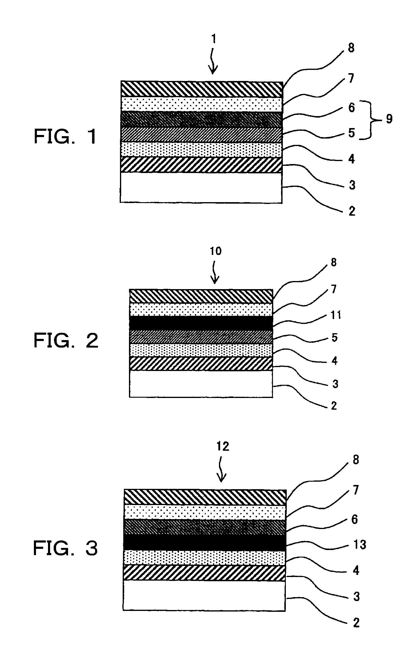
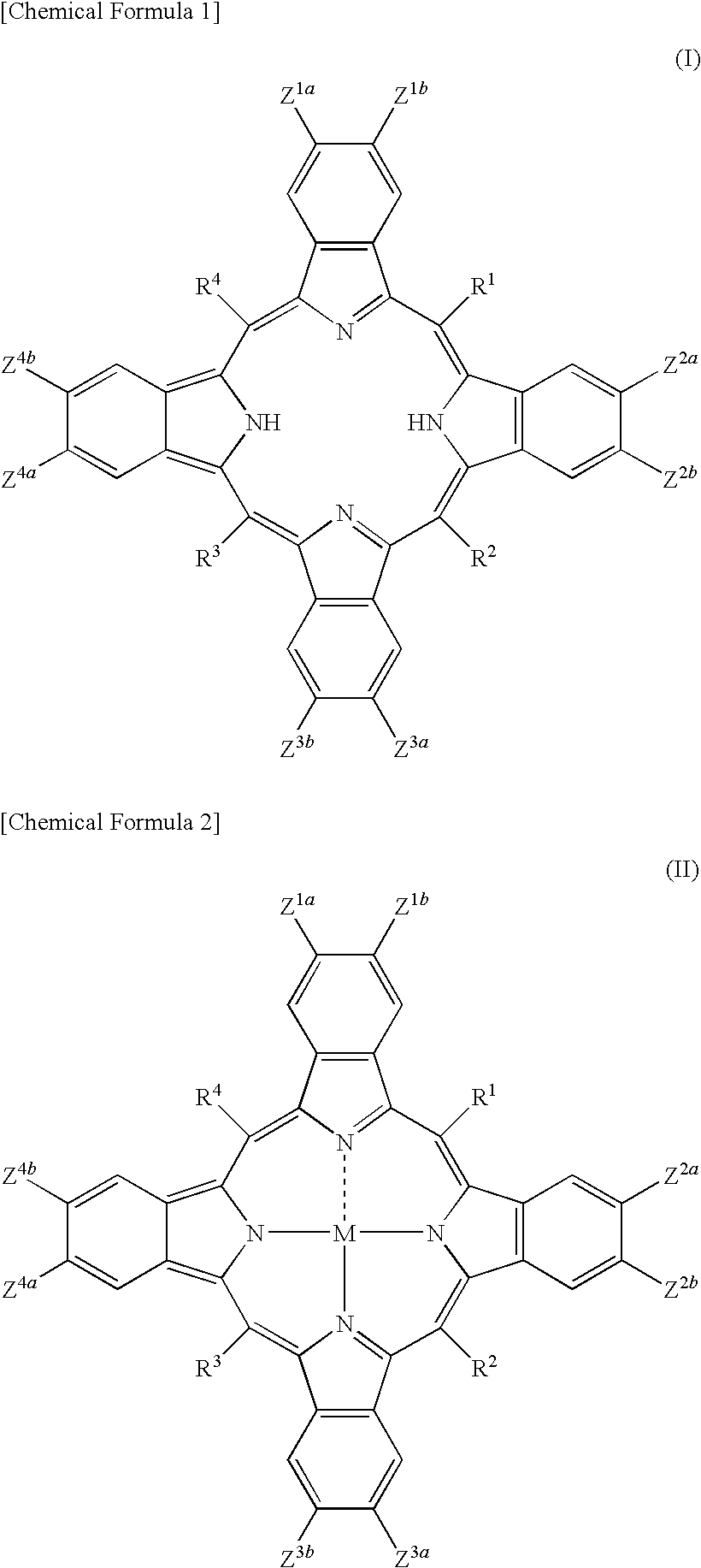
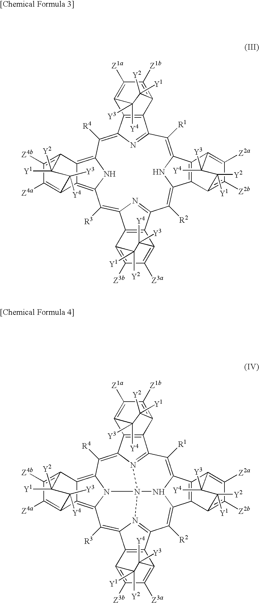
[0213]FIG. 1 is a schematic sectional view of an organic photoelectric conversion device according to a first embodiment of the present invention. As shown in FIG. 1, organic photoelectric conversion device 1 of the first embodiment includes substrate 2, positive electrode 3, p-type semiconductor layer 4, electron donor layer 5, electron acceptor layer 6, n-type semiconductor layer 7, and negative electrode B. In this organic photoelectric conversion device 1, the above electron donor layer 5 and electron acceptor layer 6 form active layer 9. In the first embodiment, active layer 9 is formed of electron donor layer 5 and electron acceptor layer 6. p-type semiconductor layer 4 and n-type semiconductor layer 7 are not essential but are preferably included. It is preferable that the first embodiment uses the benzoporphyrin compound according to the present invention as pigment. As a latent pigment corresponding to the pigment, the soluble precursor according to t...

second embodiment

[4-3. Second Embodiment]

[0296]FIG. 2 is a schematic sectional view of an organic photoelectric conversion device according to a second embodiment of the present invention. As shown in FIG. 2, organic photoelectric conversion device 10 of the second embodiment includes substrate 2, positive electrode 3, p-type semiconductor layer 4, electron donor layer 5, partial active layer 11, n-type semiconductor layer 7, and negative electrode 8. In other words, organic photoelectric conversion device 10 is identical in structure to organic photoelectric conversion device 1 of the first embodiment except that electron acceptor layer 6 is replaced by partial active layer 11. Namely, the active layer of the present embodiment is formed of an electron donor layer and partial active layer. For this reason, it is preferable that the second embodiment also uses a benzoporphyrin compound according to the present invention as the pigment similar to the first embodiment. Further, as a latent pigment cor...

third embodiment

[4-4 Third Embodiment]

[0321]FIG. 3 is a schematic sectional view of an organic photoelectric conversion device according to a third embodiment of the present invention. As shown in FIG. 3, organic photoelectric conversion device 12 of the third embodiment includes substrate 2, positive electrode 3, p-type semiconductor layer 4, partial active layer 13, electron acceptor layer 6, n-type semiconductor layer 7, and negative electrode 8. In other words, organic photoelectric conversion device 12 is identical in structure to organic photoelectric conversion device 1 of the first embodiment except that electron donor layer 5 is replaced by partial active layer 13. Namely, the active layer of the present invention is formed of partial active layer 13 and electron acceptor layer 6.

[The Substrate, the Positive Electrode, and the P-type Semiconductor Layer]

[0322]Substrate 2, positive electrode layer 3, and p-type semiconductor layer 4 are the same as those of the first embodiment.

[The Partial...


PUM

PropertyMeasurementUnit
exciton diffusion lengthaaaaaaaaaa
temperatureaaaaaaaaaa

Abstract

The objects are to provide a method for producing a durable organic photoelectric conversion device by a coating process or to produce an organic photoelectric conversion device superior in photoelectric conversion characteristics to the conventional devices. In the production method for an organic photoelectric conversion device including a substrate, a pair of electrodes which are formed on the substrate and at least one of which is transparent, and an active layer formed between the pair of electrodes, the active layer is formed by coating; and the active layer contains a pigment.

Description

CROSS-REFERENCE TO RELATED APPLICATIONS[0001]This application is a 371 of PCT / JP07 / 59338 filed May 1, 2007 and claims the benefit of JP 2006-128541 filed May 2, 2006, JP 2006-161374 filed Jun. 9, 2006 and JP 2006-321475 filed Nov. 29, 2006.TECHNICAL FIELD[0002]The present invention relates to an organic photoelectric conversion device and the production method thereof, and in particular to an organic photoelectric conversion device preferably used for an organic thin layer solar cell and an optical sensor.BACKGROUND OF THE INVENTION[0003]A conventional solar cell, one of the use of an organic photoelectric conversion device, has been developed and practically used which device is made of polycrystal silicon. The production of the device requires high purity silicon and a high-temperature process. Considering the energy required for production, the contribution to energy saving technology of solar cell has been questionable. Besides outdoor electric generation use, the conventional p...

Claims


Application Information

Patent Timeline
Patent Type & Authority Patents(United States)
IPC IPC(8): H01L31/00B82Y10/00H01L51/00H01L51/42
CPCH01L51/424B82Y10/00H01L51/0026H01L51/0078H01L51/4206H01L51/4253C08G2261/1424C08G2261/3223H01L51/009H01L51/0036H01L51/0047H01L51/0052H01L51/0053Y02E10/549Y02P70/50H10K71/40H10K85/215H10K85/113H10K85/621H10K85/311H10K85/615H10K85/361H10K30/451H10K30/20H10K30/30H10K30/00
Inventor ARAMAKI, SHINJISATO, YOSHIHARU
Owner MITSUBISHI CHEM CORP
Why Eureka
Try Eureka