Method for manufacturing photoelectric conversion device

a technology of photoelectric conversion and manufacturing method, which is applied in the field of manufacturing a photoelectric conversion device, can solve the problems of low yield of a gas needed for film formation, low productivity, and inferiority of single crystal silicon solar cells in terms of photoelectric conversion characteristics, and achieves excellent photoelectric conversion characteristics and high collection efficiency of photogenerated carriers

Inactive Publication Date: 2011-06-21
SEMICON ENERGY LAB CO LTD
View PDF127 Cites 5 Cited by
  • Summary
  • Abstract
  • Description
  • Claims
  • Application Information

AI Technical Summary

Benefits of technology

[0008]In view of the foregoing, it is an object to efficiently use silicon semiconductor materials, and to provide a method for manufacturing a photoelectric conversion device which is excellent in photoelectric conversion characteristics.
[0013]The surface of the single crystal semiconductor layer can be planarized by irradiating the surface which is exposed by separating the part of the single crystal semiconductor substrate to melt and re-single-crystallize at least a surface layer of the region irradiated with the laser beam. Furthermore, by performing a laser processing, crystal defects which remain in the single crystal semiconductor layer can be repaired. With the use of the single crystal semiconductor layer which is left over the supporting substrate by separating the part of the single crystal semiconductor substrate as a photovoltaic conversion layer, a photoelectric conversion device which is excellent in photoelectric conversion characteristics can be manufactured.
[0014]Furthermore, laser irradiation is performed to process the surface of the single crystal semiconductor layer; and then an impurity semiconductor layer is formed; thus the impurity concentration of the impurity semiconductor layer can be high, and a shallow junction can be formed. Accordingly a photovoltaic conversion device with high collection efficiency of photogenerated carriers can be manufactured.

Problems solved by technology

However, a crystal thin film silicon solar cell is still inferior to a single crystal silicon solar cell in terms of photoelectric conversion characteristics because of low crystal quality.
Further, a crystal thin film silicon solar cell has a problem in that a crystal silicon film needs to be formed by a chemical vapor deposition method to have a thickness of 1 μm or more and the productivity is low.
Furthermore, a yield of a gas needed for film formation is low; therefore, a sufficient advantage in a crystal thin film silicon solar cell has not also been found from an economic stand point.
In other words, in a crystal thin film silicon solar cell, a photoelectric conversion layer is formed by a deposition technique such as a plasma CVD method; however, it is necessary that a large amount of semiconductor material gas flow for increasing deposition speed, resulting in a problem of low productivity.
On the other hand, the demand of the silicon wafer is tightened, and thus, there is a problem that the supply cannot keep up with the demand.

Method used


Image

  • Method for manufacturing photoelectric conversion device
  • Method for manufacturing photoelectric conversion device
  • Method for manufacturing photoelectric conversion device

Examples


embodiment mode 1

[0056]In this embodiment mode, a method for manufacturing a photovoltaic conversion device using a solar cell by separating a thin single crystal semiconductor layer from a single crystal semiconductor substrate and transferring the separated single crystal semiconductor layer to a substrate having an insulating surface or an insulating substrate, will be described with reference to the drawings.

[0057]FIG. 7 is a plan view of a photovoltaic conversion device 10 according to this embodiment mode. This photovoltaic conversion device 10 generates electric power when light is incident on a single crystal semiconductor layer 112 provided over a supporting substrate 105. In the single crystal semiconductor layer 112, an impurity semiconductor layer for forming a built-in electric field is formed. As the single crystal semiconductor layer 112, typically, single crystal silicon is used. Further, a polycrystalline semiconductor layer can be used instead of the single crystal semiconductor la...

embodiment mode 2

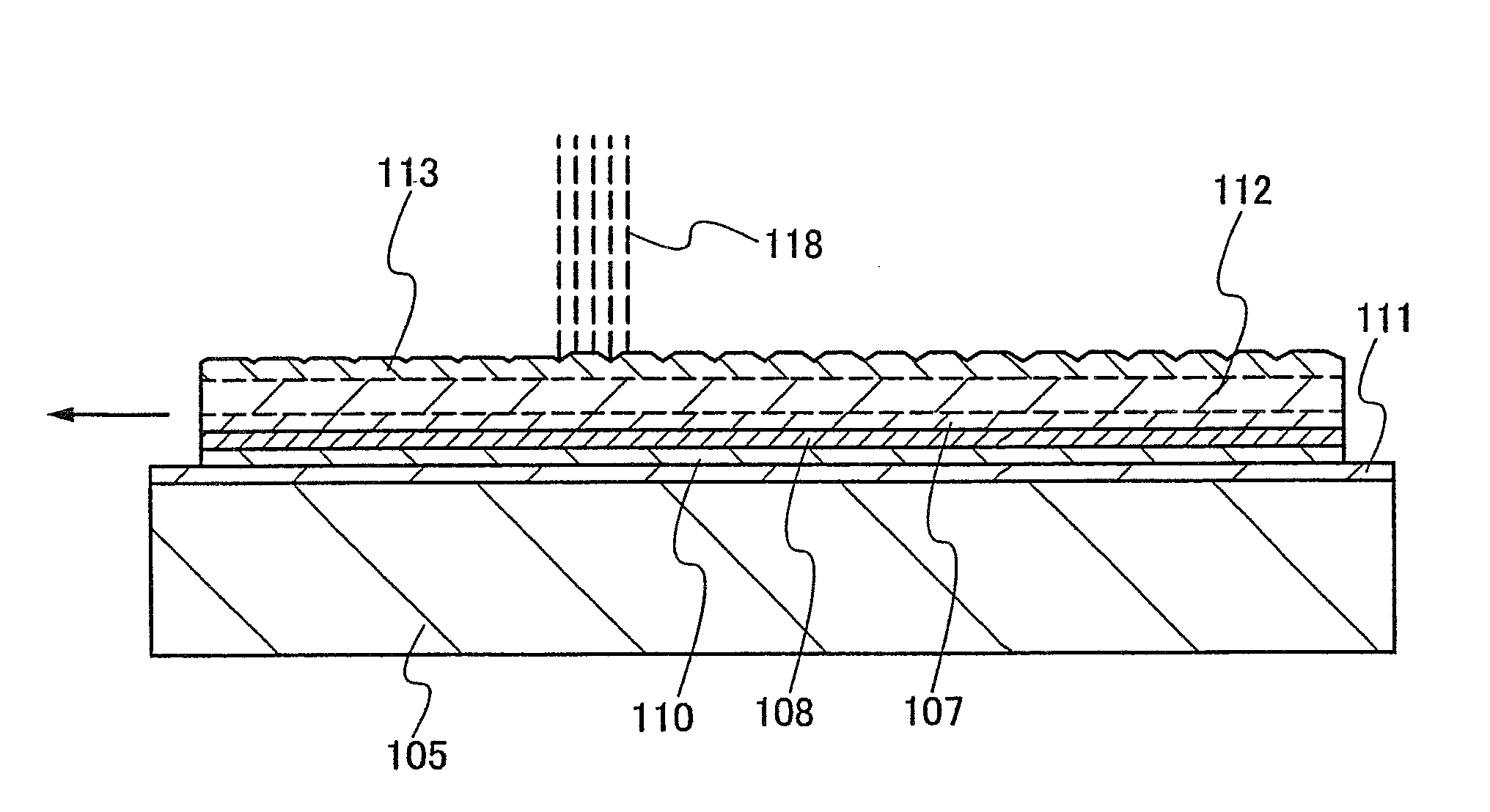
[0096]In this embodiment mode, a manufacturing process which is different from that in Embodiment Mode 1 is shown with reference to FIGS. 16A to 16C. As shown in FIG. 16A, the protective film 106 is formed over the semiconductor substrate 101 for transfer, an impurity imparting one conductivity type is added through the protective film 106 to form the first impurity semiconductor layer 107, and then, cluster ions of hydrogen are introduced with the protective film 106 left so as to form the damaged layer 109. Thereafter, as shown in FIG. 16C, the protective film 106 is removed and the first electrode 108 is formed.

[0097]By the above-described process, the protective film 106 can be effectively utilized as an anti-damage layer in ion doping. That is, by removing the protective film 106 that is damaged due to ion irradiation before forming the first electrode 108, the surface of the semiconductor substrate 101 for transfer can be prevented from being damaged. Moreover, cluster ions of...

embodiment mode 3

[0098]In this embodiment mode, a manufacturing process which is different from that in Embodiment Mode 1 is shown with reference to FIGS. 17A to 17C. As shown in FIG. 17A, the first electrode 108 is formed over the semiconductor substrate 101 for transfer, and as shown in FIG. 17B, an impurity imparting one conductivity type is added through the first electrode 108 so as to form the first semiconductor layer 107. Then, as shown in FIG. 17C, cluster ions of hydrogen are introduced through the first electrode 108 and the first impurity semiconductor layer 107 to form the damaged layer 109.

[0099]In this process, the first impurity semiconductor layer 107 is formed through the first electrode 108; thus the thickness of the first impurity semiconductor layer 107 can be controlled easily. Furthermore, the damaged layer 109 is formed after forming the first electrode 108; therefore, the first electrode 108 can be used as an anti-damage layer in ion doping. Accordingly, a step of forming a ...


PUM


Abstract

A photoelectric conversion device which is excellent in photoelectric conversion characteristics is provided by effectively utilizing silicon semiconductor materials. The present invention relates to a method for manufacturing a photoelectric conversion device using a solar cell, in which a plurality of single crystal semiconductor substrates in each of which a damaged layer is formed at a predetermined depth is arranged over a supporting substrate having an insulating surface; a surface layer part of the single crystal semiconductor substrate is separated thinly using the damaged layer as a boundary so as to form a single crystal semiconductor layer over one surface of the supporting substrate; and the single crystal semiconductor layer is irradiated with a laser beam from a surface side which is exposed by separation of the single crystal semiconductor layer to planarize the surface of the single crystal semiconductor layer.

Description

TECHNICAL FIELD[0001]The present invention relates to a method for manufacturing a photoelectric conversion device using a semiconductor layer, and particularly relates to a photoelectric conversion device using a single crystal semiconductor layer.BACKGROUND ART[0002]As a measure against global warming, solar photovoltaics become popular around the world. The total production of solar cells in the world in 2005 was 1, 759 MW, which is an increase by 147% over the previous fiscal year. At present, the popular solar cell is crystal solar cells, and solar cells using single crystal silicon or polycrystalline silicon account for the large part of the production. These solar cells use a silicon wafer as a base, which is formed by slicing a large-sized silicon ingot into a circle.[0003]In a crystal solar cell using silicon as a material, a thickness of a silicon wafer which is sufficient to absorb sun light is about 10 μm. However, an actual silicon wafer has a thickness of about 200 μm ...

Claims


Application Information

Patent Timeline
Patent Type & Authority Patents(United States)
IPC IPC(8): H01L21/00
CPCH01L21/76254H01L31/1892H01L31/1804Y02E10/547Y02P70/50
Inventor YAMAZAKI, SHUNPEIARAI, YASUYUKI
Owner SEMICON ENERGY LAB CO LTD
Why Eureka
Try Eureka