Display device with clearance

a technology of display device and clearance, which is applied in the direction of solid-state device, spectral modifier, light and heating apparatus, etc., to achieve the effect of disrupting the luminance balance and improving the efficiency of light extraction

Active Publication Date: 2015-09-22
SONY CORP
View PDF9 Cites 5 Cited by
  • Summary
  • Abstract
  • Description
  • Claims
  • Application Information

AI Technical Summary

Benefits of technology

[0004]However, such a previous display device has had a difficulty that when a view angle characteristic is varied between colors, white balance is disrupted, and therefore chromaticity of white or and intermediate color is changed depending on view angles. A major cause of...

Problems solved by technology

However, such a previous display device has had a difficulty that when a view angle characteristic is varied between color...

Method used


Image

  • Display device with clearance
  • Display device with clearance
  • Display device with clearance

Examples


embodiment

1. Embodiment

[0039](1) Description of the principle (example where width of emission regions are the same between all colors, and a blue clearance is large compared with that for another color)[0040](2) Calculation example 1 (example where width of emission regions are the same between all colors, and a blue clearance is small compared with that for another color)[0041](3) Calculation example 2 (example where width of a blue emission region is large compared with width of another color emission region, and a blue clearance is small compared with that for another color)

2. Modification 1 (Example where a Clearance is Continuously Changed within One Self-Luminous Element)

3. Application Examples

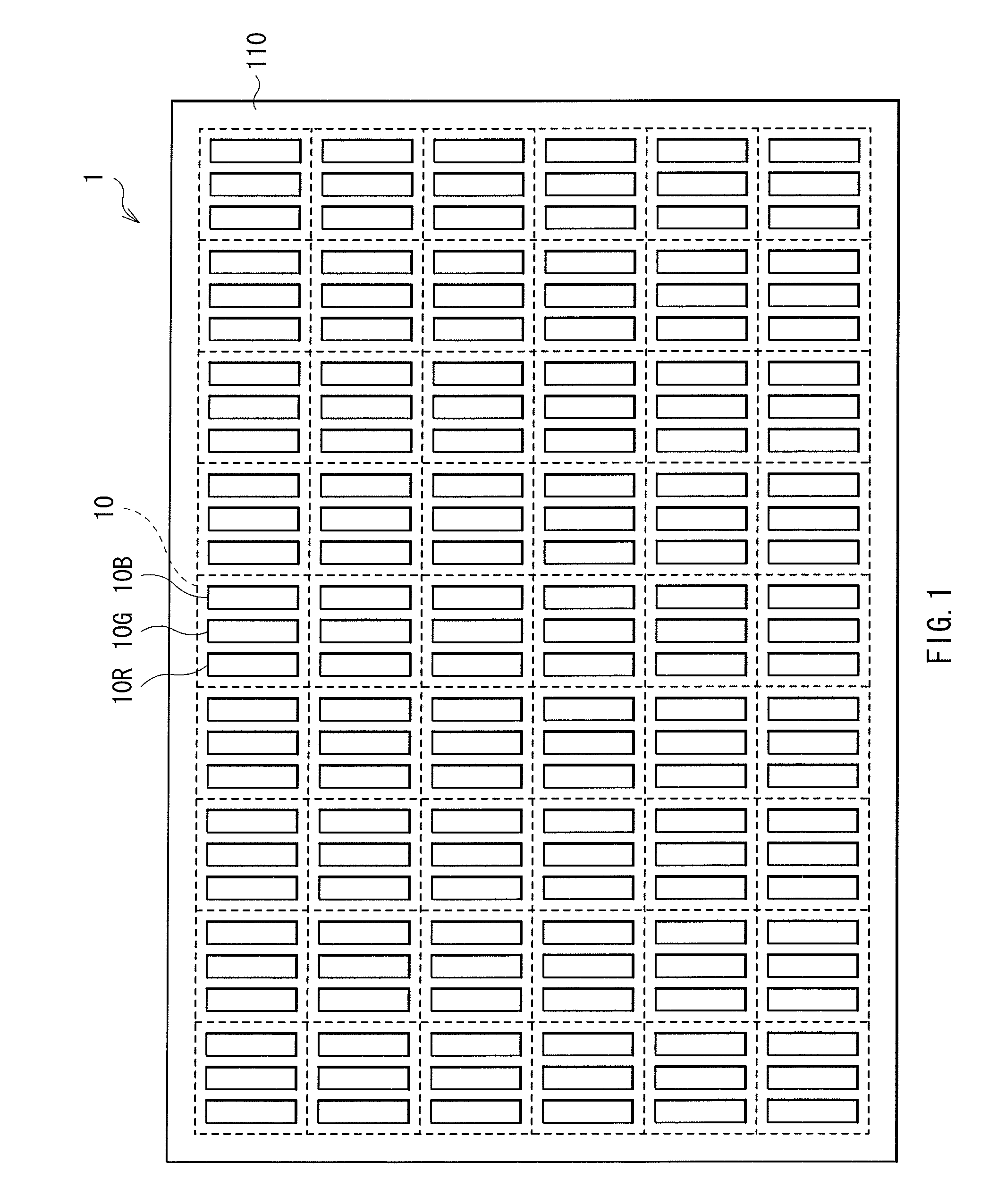
[0042]FIG. 1 shows an example of a planar configuration of a display device according to an embodiment. The display device 1 is used for a television apparatus or the like, and has a configuration where a plurality of pixels 10 are arranged, for example, in a matrix in a display region 110. Each ...

example 1

Calculation Example 1

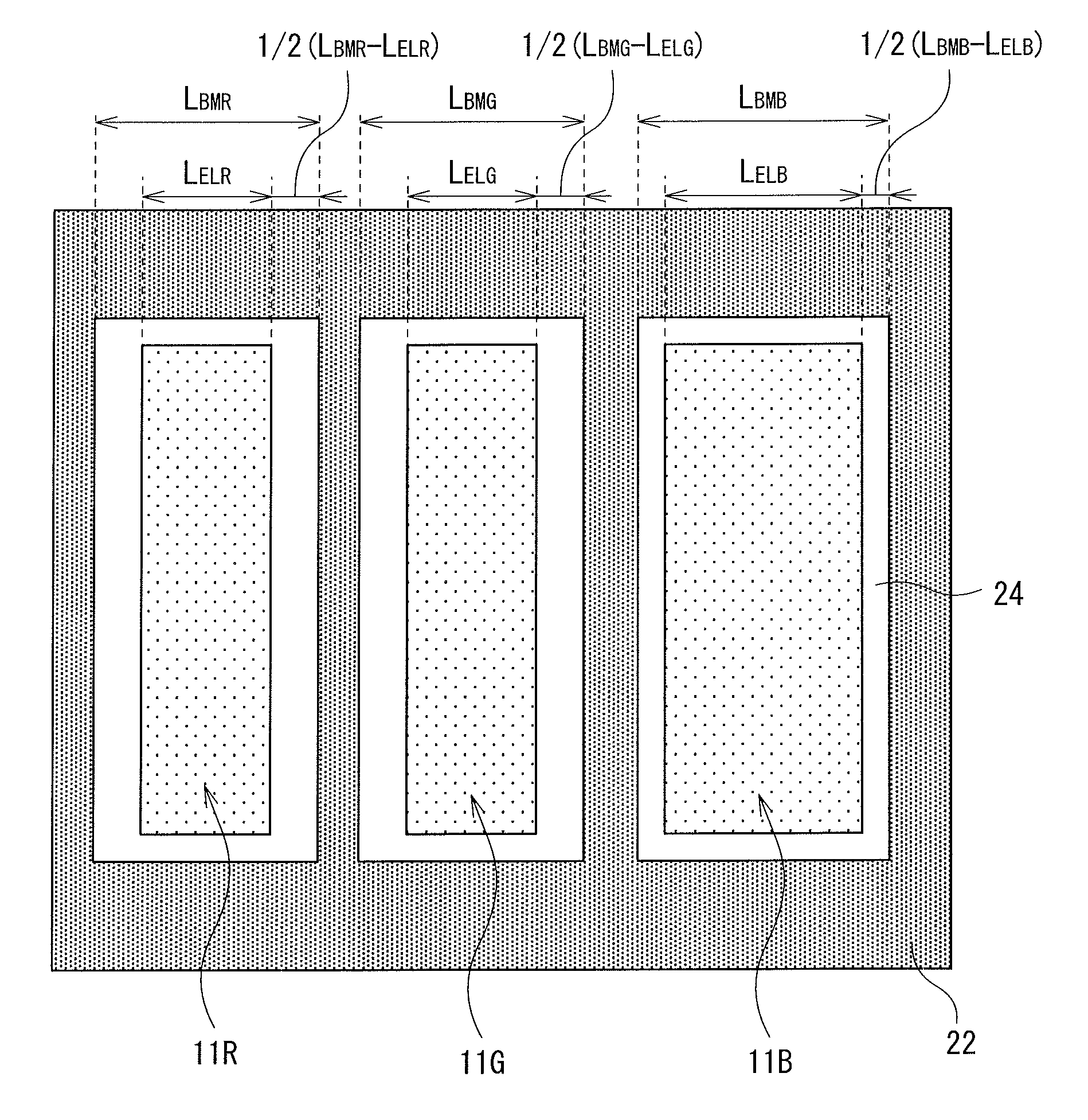
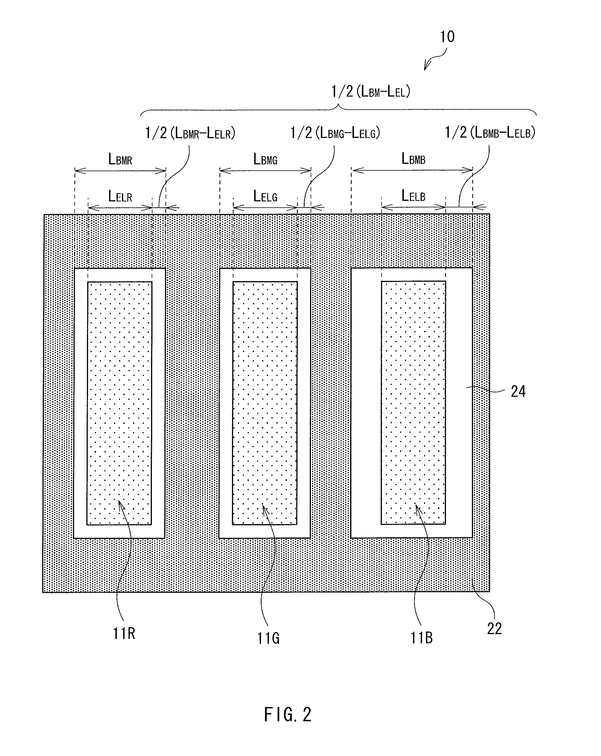
[0064]FIGS. 4 and 5 show a planar configuration and a sectional configuration of a pixel 10 according to calculation example 1, respectively. In the calculation example 1, as shown in FIG. 4, while widths of the emission regions 11R, 11G and 11B are the same between all colors, width LBMB of the opening 24 facing the blue emission region 11B is smaller than widths LBMR and LBMG of the openings 24 facing the red and green emission regions 11R and 11G. Accordingly, the clearance, ½(LBMB−LELB), of the blue self-luminous element 10B is smaller than the clearances, ½(LBMR−LELR) and ½(LBMG−LELG), of the red and green self-luminous elements 10R and 10G. These are summarized in numerical expression 7.

Width of emission region: LELR=LELG=LELB=60 μm

Width of opening: LBMR=LBMG=76 μm,LBMB=70 μm

Red clearance: ½(LBMR−LELR)=8 μm

Green clearance: ½(LBMG−LELG)=8 μm

Blue clearance: ½(LBMB−LELB)=5 μm  Numerical expression 7

[0065]FIG. 6 shows a calculation result of a chromaticity-to-...

example 2

Calculation Example 2

[0068]FIGS. 8 and 9 show a planar configuration and a sectional configuration of a pixel 10 according to calculation example 2. In the calculation example 2, as shown in FIG. 8, width LELB of the blue emission region 11B is larger than widths LLER and LLEG of the red and green emission regions 11R and 11G. In addition, width LBMB of the opening 24 facing the blue emission region 11B is larger than widths LBMR and LBMG of the openings 24 facing the red and green emission regions 11R and 11G. Accordingly, the clearance, ½(LBMB−LELB), of the blue self-luminous element 10B is smaller than the clearances, ½(LBMR−LELR) and ½(LBMG−LELG), of the red and green self-luminous elements 10R and 10G. These are summarized in numerical expression 8.

Width of emission region: LELR=LELG=50 μm,LELB=74 μm

Width of opening: LBMR=LBMG=66 μm,LBMB=84 μm

Red clearance: ½(LBMR−LELR)=8 μm

Green clearance: ½(LBMG−LELG)=8 μm

Blue clearance: ½(LBMB−LELB)=5 μm  Numerical expression 8

[0069]The reas...


PUM


Abstract

A display device is provided, in which view-angle dependence of chromaticity of white or an intermediate color may be reduced. The display device includes a pair of opposed substrates, a light blocking layer provided on one of the pair of substrates while having a plurality of openings, and a plurality of self-luminous elements provided on the other of the pair of substrates, each of the self-luminous elements having an emission region facing each of the openings, and having an emission color different from an emission color of another element, at least one self-luminous element being different from other self-luminous elements in clearance in a display plane direction from an end of the emission region to an opening of the light blocking film.

Description

CROSS REFERENCES TO RELATED APPLICATIONS[0001]This application is a continuation application of, and claims the benefit of and priority to, U.S. patent application Ser. No. 13 / 744,036, filed Jan. 17, 2013, which is a continuation of U.S. patent application Ser. No. 12 / 849,912, filed on Aug. 4, 2010, now U.S. Pat. No. 8,395,308, issued Mar. 12, 2013, which claims priority to Japanese Priority Patent Application JP 2009-189445, filed in the Japanese Patent Office on Aug. 18, 2009, the entire contents of each of which are hereby incorporated by reference.BACKGROUND[0002]The present application relates to a display device having self-luminous elements such as organic EL (Electroluminescence) elements or inorganic EL elements.[0003]In the display device using self-luminous elements such as organic EL elements, the self-luminous elements are provided on one of a pair of substrates, and a light blocking black matrix is provided on the other (for example, see Japanese Patent Application, Pu...

Claims


Application Information

Patent Timeline
IPC IPC(8): F21V9/00H01L27/32H01L51/52
CPCF21V9/00H01L27/322H01L27/3211H01L27/3216H01L51/5284H01L27/3206H01L51/5265H10K59/30H10K59/352H10K59/876H10K59/8792H10K59/35H10K50/865H10K59/38H10K50/852
Inventor ASAKI, REO
Owner SONY CORP
Why Eureka
Try Eureka