Display device and manufacturing method thereof
a technology of display device and manufacturing method, which is applied in the field of display device, can solve the problems of driving voltage and hysteresis which remain issues to be solved, and the operating temperature range of only 1k of blue phase liquid crystals, so as to reduce the driving voltage of the display device, reduce the effect of transmittance and effective increas
- Summary
- Abstract
- Description
- Claims
- Application Information
AI Technical Summary
Benefits of technology
Problems solved by technology
Method used
Image

Examples
first embodiment
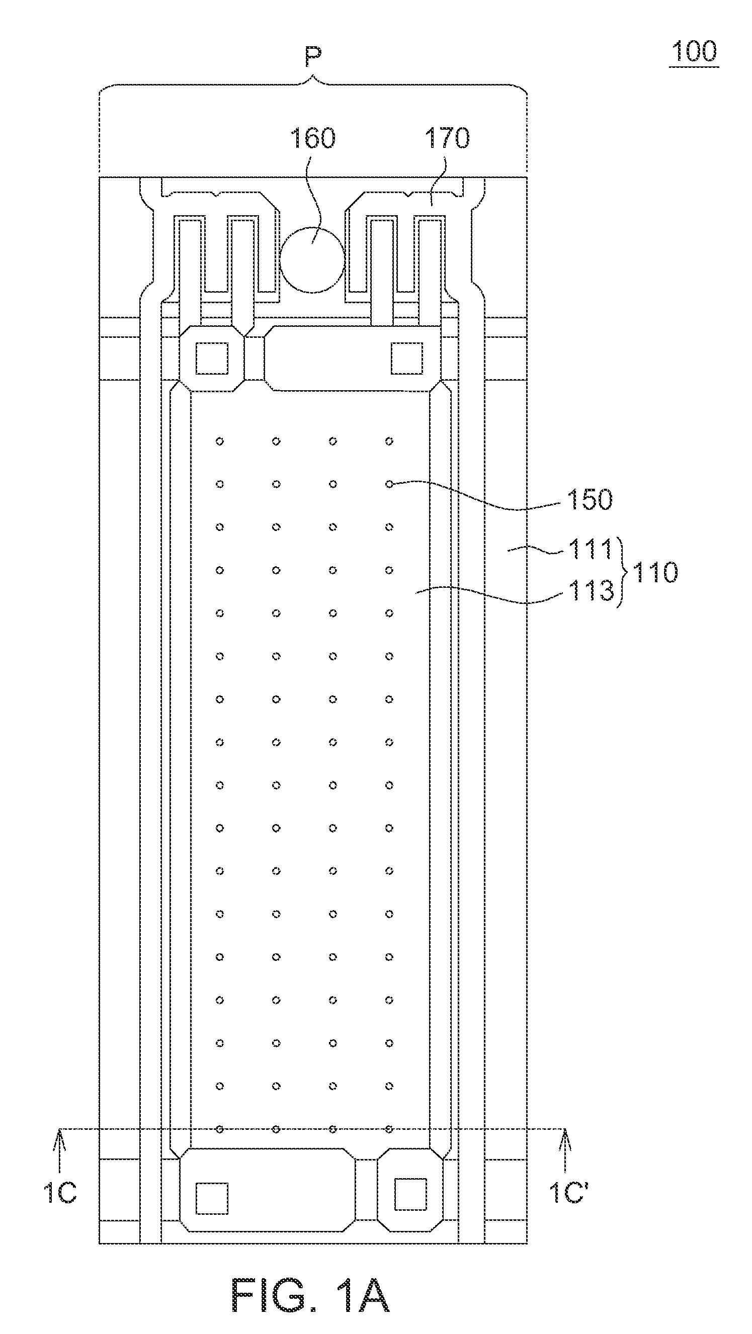
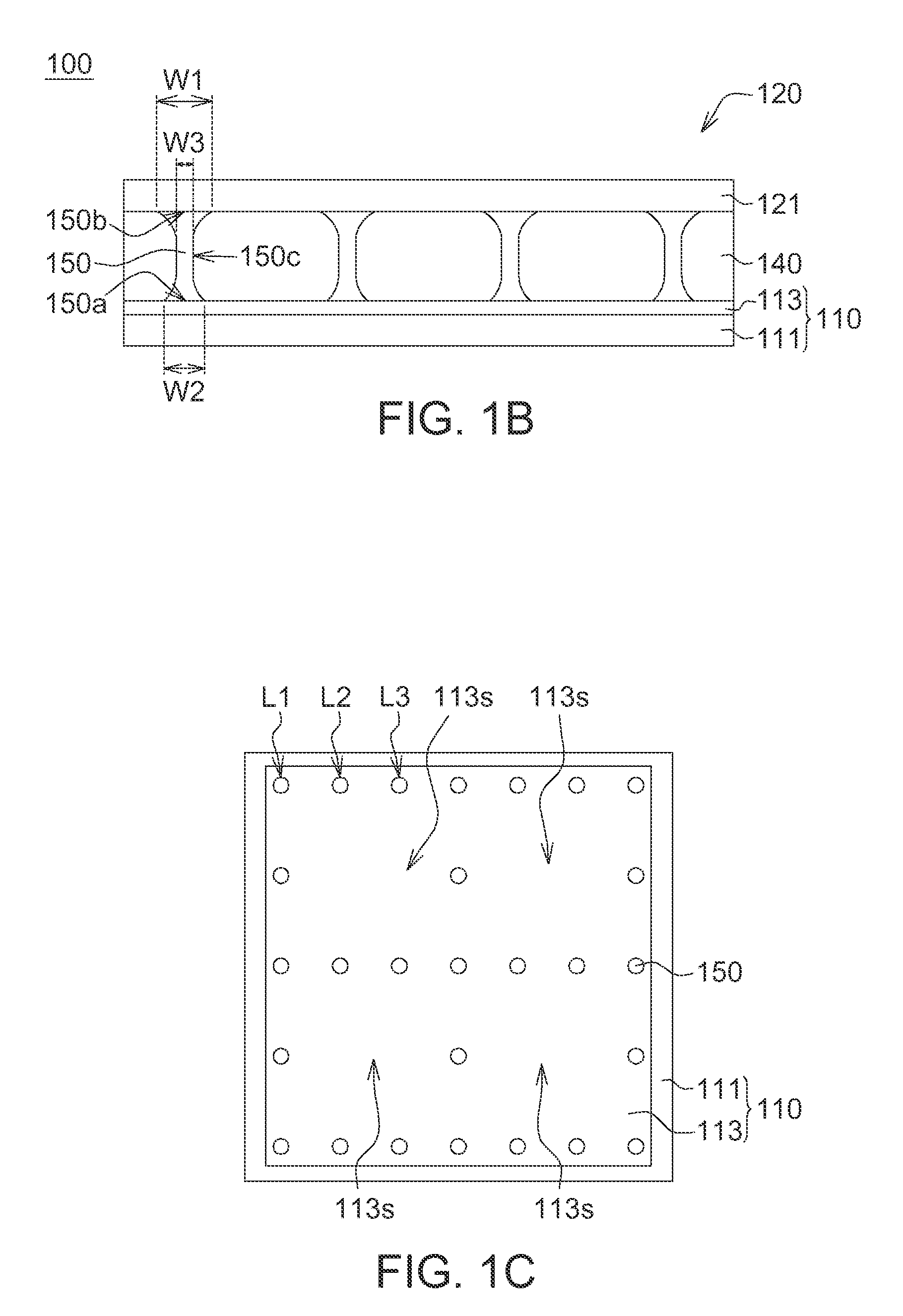
[0025]FIG. 1A shows a schematic diagram of a display device according to the present invention; FIG. 1B shows a sectional view along a section line 1C-1C′ in FIG. 1A. Referring to FIGS. 1A and 1B, a display device 100 has a plurality of pixel units P. In FIG. 1A, one of the pixel units P is depicted. The display device 100 includes a first substrate assembly 110, a second substrate assembly 120, a liquid crystal mixture 140, and a pillared polymer network 150. The first substrate assembly 110 includes a first substrate 111 and a first electrode layer 113 disposed on the first substrate 111. The second substrate assembly 120 includes a second substrate 121. The liquid crystal mixture 140 is disposed between the first substrate assembly 110 and the second substrate assembly 120. The pillared polymer network 150 is disposed between the first substrate assembly 110 and the second substrate assembly 120, and the pillared polymer network 150 has a first end 150a and a second end 150b. The...
second embodiment
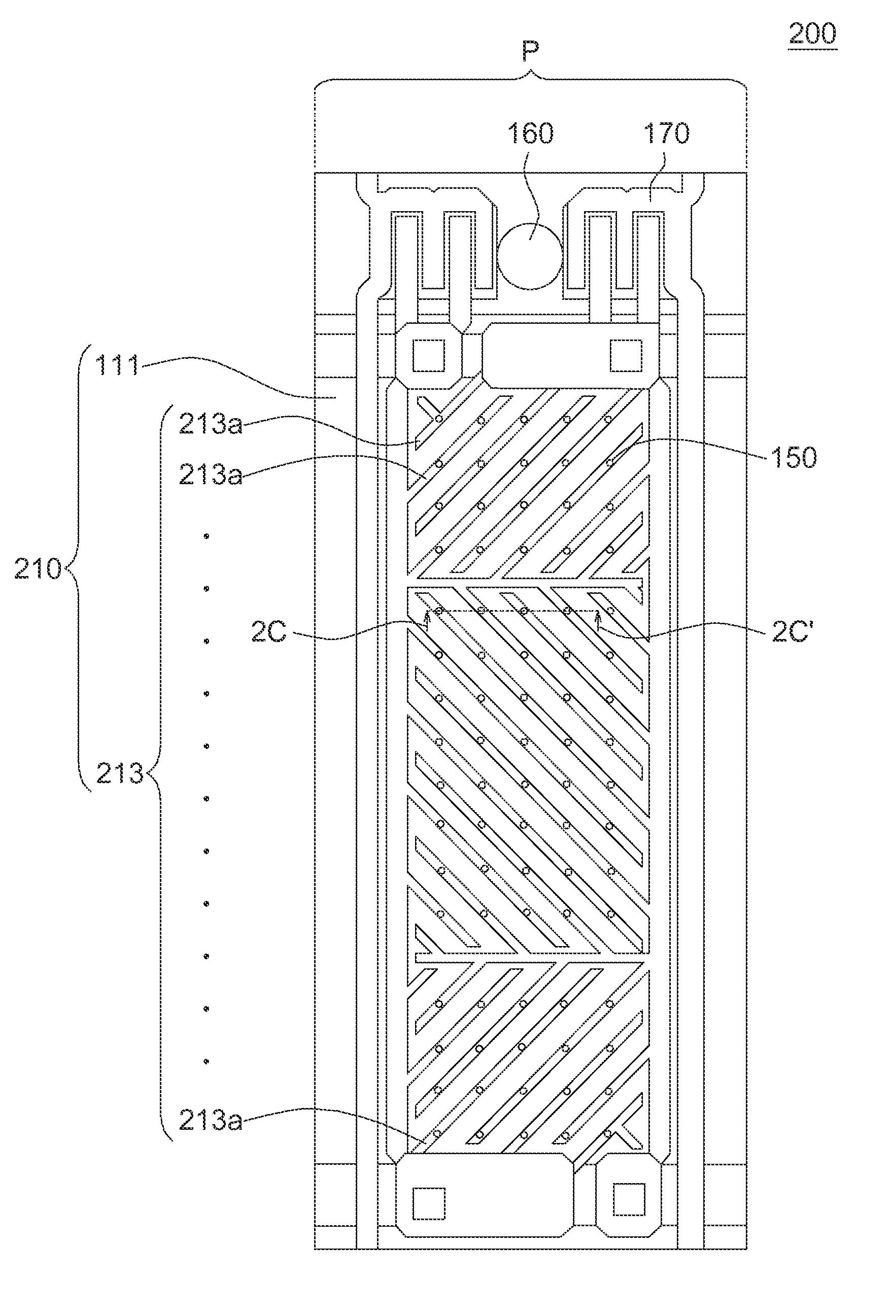
[0035]FIG. 2A shows a schematic diagram of a display device according to the present invention; FIG. 2B shows a sectional view along a section line 2C-2C′ in FIG. 2A. A display device 200 includes a plurality of pixel units P. In FIG. 2A, one of the pixel units P is depicted. Same elements in this embodiment and the foregoing embodiment inherit the same denotations. Details of the same elements can be referred in the foregoing descriptions, and shall be omitted herein.
[0036]The display device 200 includes a first substrate assembly 210, a second substrate assembly 120, a liquid crystal mixture 140, and a pillared polymer network 150. The first substrate assembly 210 includes a first substrate 111 and a first electrode layer 213 disposed on the first substrate 111. The first electrode layer 213 includes a plurality of first electrode strips 213a, and first end 150a of the pillared polymer network 150 is disposed correspondingly to the first electrode strips 213a. In an embodiment, fo...
third embodiment
[0040]FIG. 3 shows a sectional view of a display device according to the present invention. Same elements in this embodiment and the foregoing embodiment inherit the same denotations. Details of the same elements can be referred in the foregoing descriptions, and shall be omitted herein.
[0041]A display device 300 includes a first substrate assembly 110, a second substrate assembly 320, a liquid crystal mixture 140, and a pillared polymer network 150. The first substrate assembly 110 includes a first substrate 111 and a first electrode layer 113 disposed on the first substrate 111. The second substrate assembly 320 includes a second substrate 121 and a second electrode layer 323 disposed on the second substrate 121. The first end 150a of the pillared polymer network 150 abuts against the first substrate assembly 110. The second end 150b of the pillared polymer network 150 abuts against the second substrate assembly 120 and is disposed correspondingly to the second electrode layer 323...
PUM
| Property | Measurement | Unit |
|---|---|---|
| length | aaaaa | aaaaa |
| width | aaaaa | aaaaa |
| distance | aaaaa | aaaaa |
Abstract
Description
Claims
Application Information
 - R&D
- Intellectual Property
- Life Sciences
- Materials
- Tech Scout
- Unparalleled Data Quality
- Higher Quality Content
- 60% Fewer Hallucinations
Browse by: Latest US Patents, China's latest patents, Technical Efficacy Thesaurus, Application Domain, Technology Topic, Popular Technical Reports.
© 2025 PatSnap. All rights reserved.Legal|Privacy policy|Modern Slavery Act Transparency Statement|Sitemap|About US| Contact US: help@patsnap.com