Integrated electro-absorption modulator

a modulator and electro-absorption technology, applied in the direction of instruments, final product manufacturing, sustainable manufacturing/processing, etc., can solve the problems of complex and poor performance of the attempts to integrate in-plane fk and qcse electro-absorption modulators in optical waveguides on soi substrates, and the high voltage typically required during the operation of these optical devices

Active Publication Date: 2015-09-22
ORACLE INT CORP
View PDF3 Cites 21 Cited by
  • Summary
  • Abstract
  • Description
  • Claims
  • Application Information

AI Technical Summary

Benefits of technology

[0014]In some embodiments, the optical device includes inverse optical tapers defined in the germanium, where the inverse optical tapers control a spatial extent of an optical mode in the germanium. The inverse optical tapers may include doped regions in the germanium.

Problems solved by technology

However, in practice a surface-normal device geometry often requires thick active layers (in order for the light to interact with the silicon-germanium layer).
Therefore, very high voltage is typically needed during operation of these optical devices.
Furthermore, these optical devices usually are not compatible with the in-plane, edge geometries that are typically used for optical-waveguide operation.
For example, attempts at integrating in-plane FK and QCSE electro-absorption modulators in optical waveguides on SOI substrates are typically complicated and usually have poor performance.

Method used


Image

  • Integrated electro-absorption modulator
  • Integrated electro-absorption modulator
  • Integrated electro-absorption modulator

Examples


Embodiment Construction

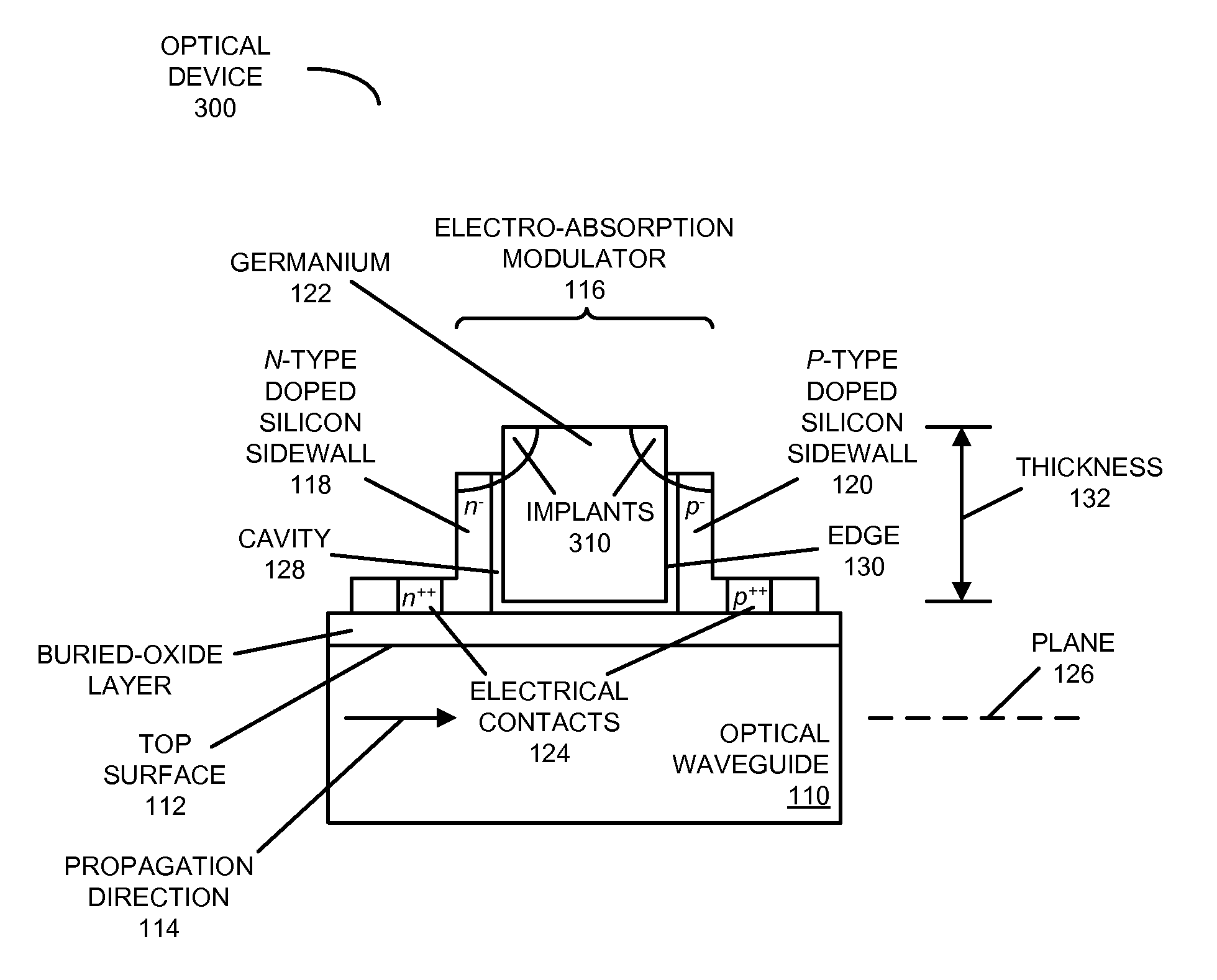
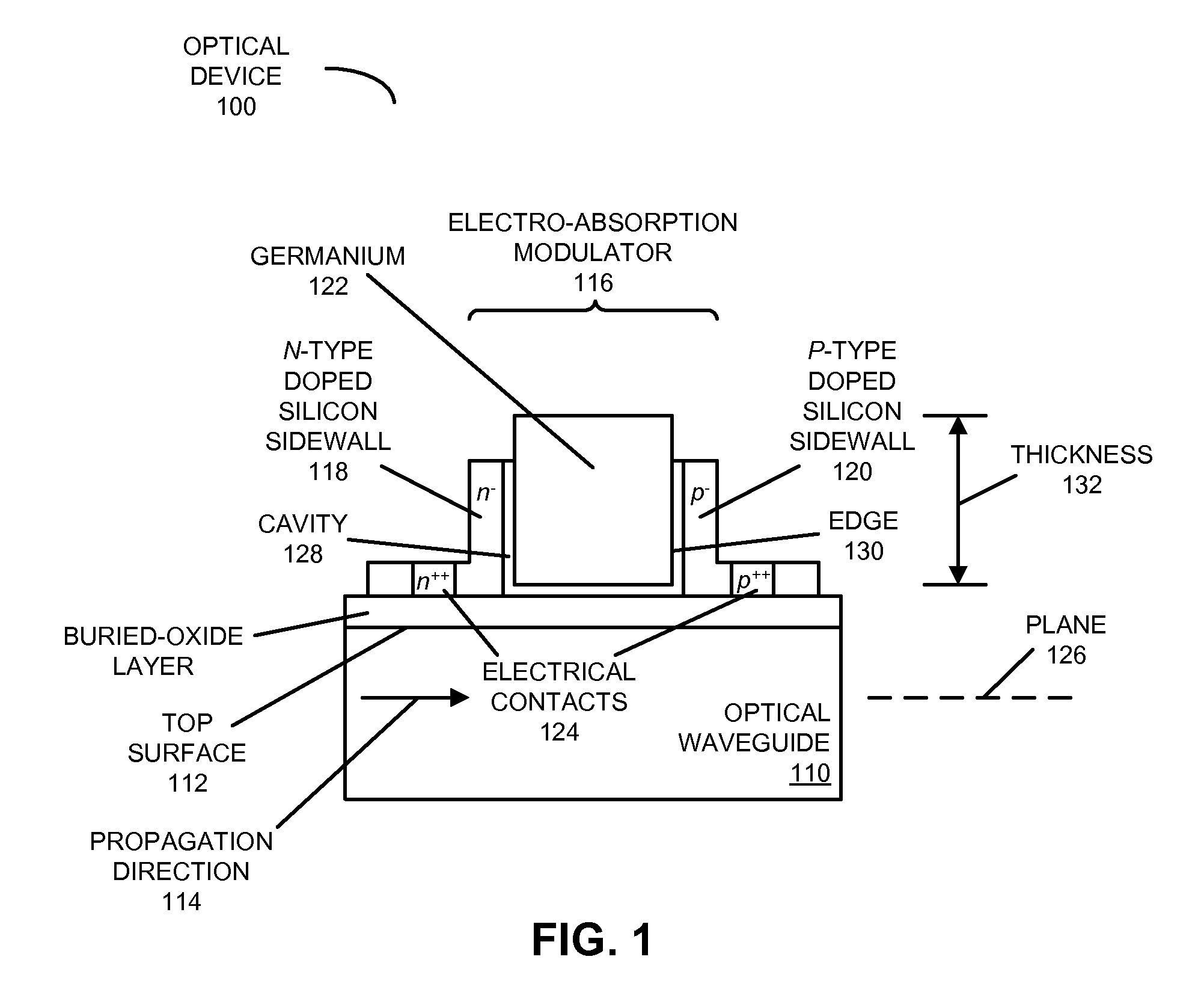
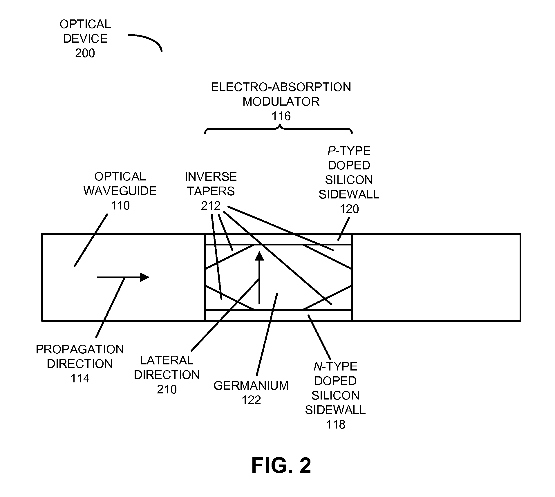
[0028]Embodiments of an optical device, a system that includes the optical device, and a method for modulating an optical signal are described. This integrated optical device includes an electro-absorption modulator disposed on a top surface of an optical waveguide. The electro-absorption modulator includes germanium disposed in a cavity between an n-type doped silicon sidewall and a p-type doped silicon sidewall. By applying a voltage between the n-type doped silicon sidewall and the p-type doped silicon sidewall, an electric field can be generated in a plane of the optical waveguide, but perpendicular to a propagation direction of the optical signal. This electric field shifts a band gap of the germanium, thereby modulating the optical signal.

[0029]The electro-absorption modulator on silicon in the optical device operates at low voltage and can be integrated with a silicon optical waveguide on a silicon-on-insulator (SOI) platform. Moreover, the optical device is compatible with C...


PUM


Abstract

An integrated optical device includes an electro-absorption modulator disposed on a top surface of an optical waveguide. The electro-absorption modulator includes germanium disposed in a cavity between an n-type doped silicon sidewall and a p-type doped silicon sidewall. By applying a voltage between the n-type doped silicon sidewall and the p-type doped silicon sidewall, an electric field can be generated in a plane of the optical waveguide, but perpendicular to a propagation direction of the optical signal. This electric field shifts a band gap of the germanium, thereby modulating the optical signal.

Description

GOVERNMENT LICENSE RIGHTS[0001]This invention was made with United States government support under Agreement No. HR0011-08-9-0001 awarded by DARPA. The United States government has certain rights in the invention.BACKGROUND[0002]1. Field[0003]The present disclosure relates to techniques for modulating optical signals. More specifically, the present disclosure relates to an integrated optical device that includes an electro-absorption modulator.[0004]2. Related Art[0005]Silicon photonics is a promising technology that can provide large communication bandwidth, low latency and low power consumption for inter-chip and intra-chip optical interconnects or links. A key component for use in inter-chip and intra-chip optical interconnects is a modulator that can be monolithically integrated into the same silicon layer as transistors and other optical components.[0006]Some approaches for implementing silicon-photonic modulators are based on germanium, which is an efficient absorbing material...

Claims


Application Information

Patent Timeline
Patent Type & Authority Patents(United States)
IPC IPC(8): H01L31/18H01L31/0232
CPCH01L31/02327G02F1/0018G02F1/015G02F1/025H01L21/26513G02B6/12G02B2006/12107G02B2006/12142G02F1/0157Y02P70/50
Inventor CUNNINGHAM, JOHN E.YAO, JINSHUBIN, IVANLI, GUOLIANGZHENG, XUEZHELIN, SHIYUNTHACKER, HIREN D.DJORDJEVIC, STEVAN S.KRISHNAMOORTHY, ASHOK V.
Owner ORACLE INT CORP
Why Eureka
Try Eureka