Semiconductor device

Inactive Publication Date: 2015-10-27
KK TOSHIBA
View PDF13 Cites 1 Cited by
  • Summary
  • Abstract
  • Description
  • Claims
  • Application Information

AI Technical Summary

Benefits of technology

The semiconductor device described in this patent helps to reduce the resistance of the packaged device, improve production efficiency, and prevent thermal degradation. It does this by increasing the contact area between the lead frame contact plate and the source terminal, which allows for a larger path of electric current flow. By doing so, the device reduces the resistance of the electric current and achieves lower package resistance.

Problems solved by technology

However, the sizes of semiconductor chips may be different and thus the contact area of the standard connector may not be suitable for connection with differently sized semiconductor chips.
This may result in increased resistance between an external electrode and the semiconductor chip, which may cause degradation of the semiconductor chip performance.

Method used


Image

  • Semiconductor device
  • Semiconductor device
  • Semiconductor device

Examples


first embodiment

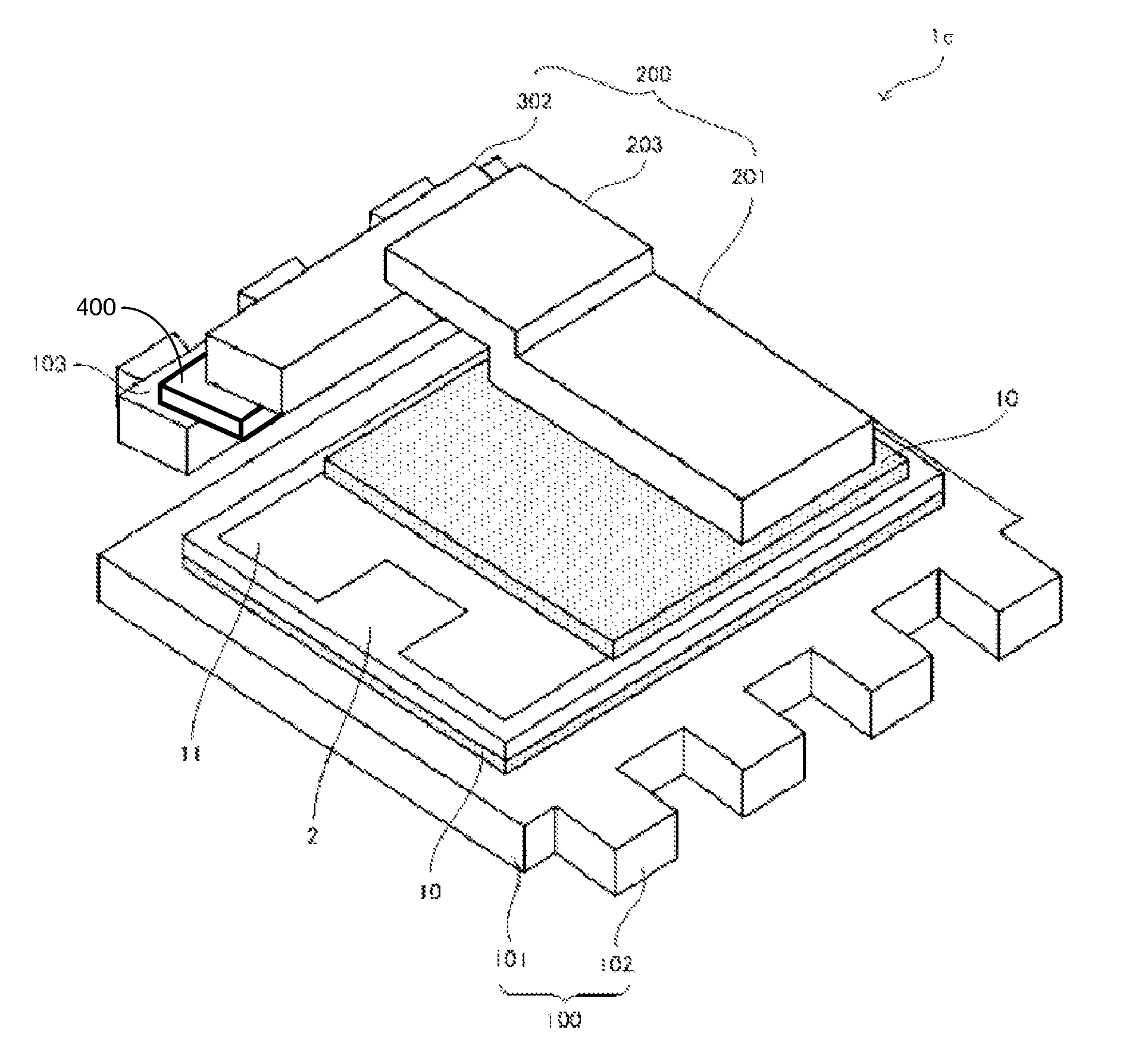
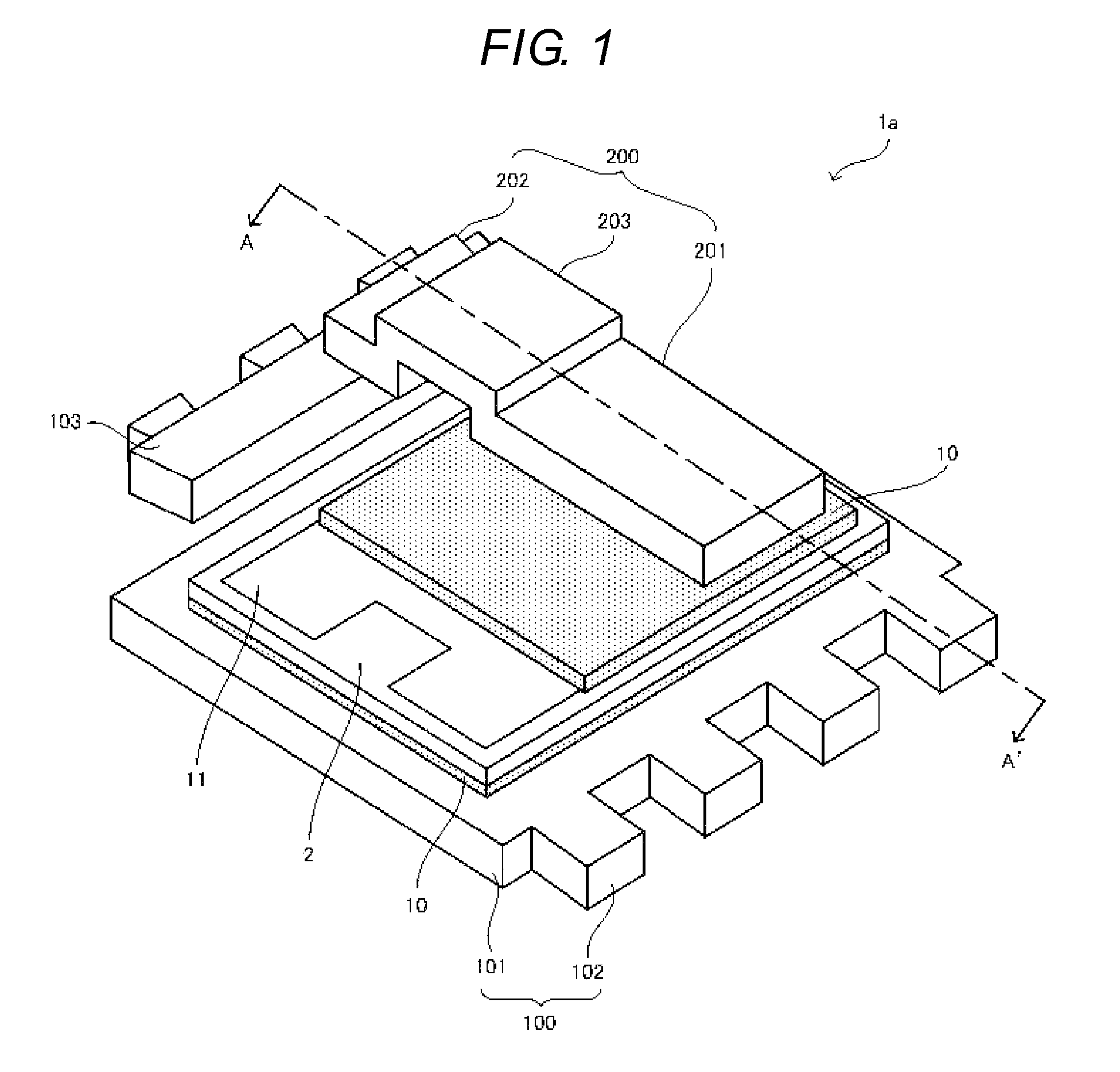
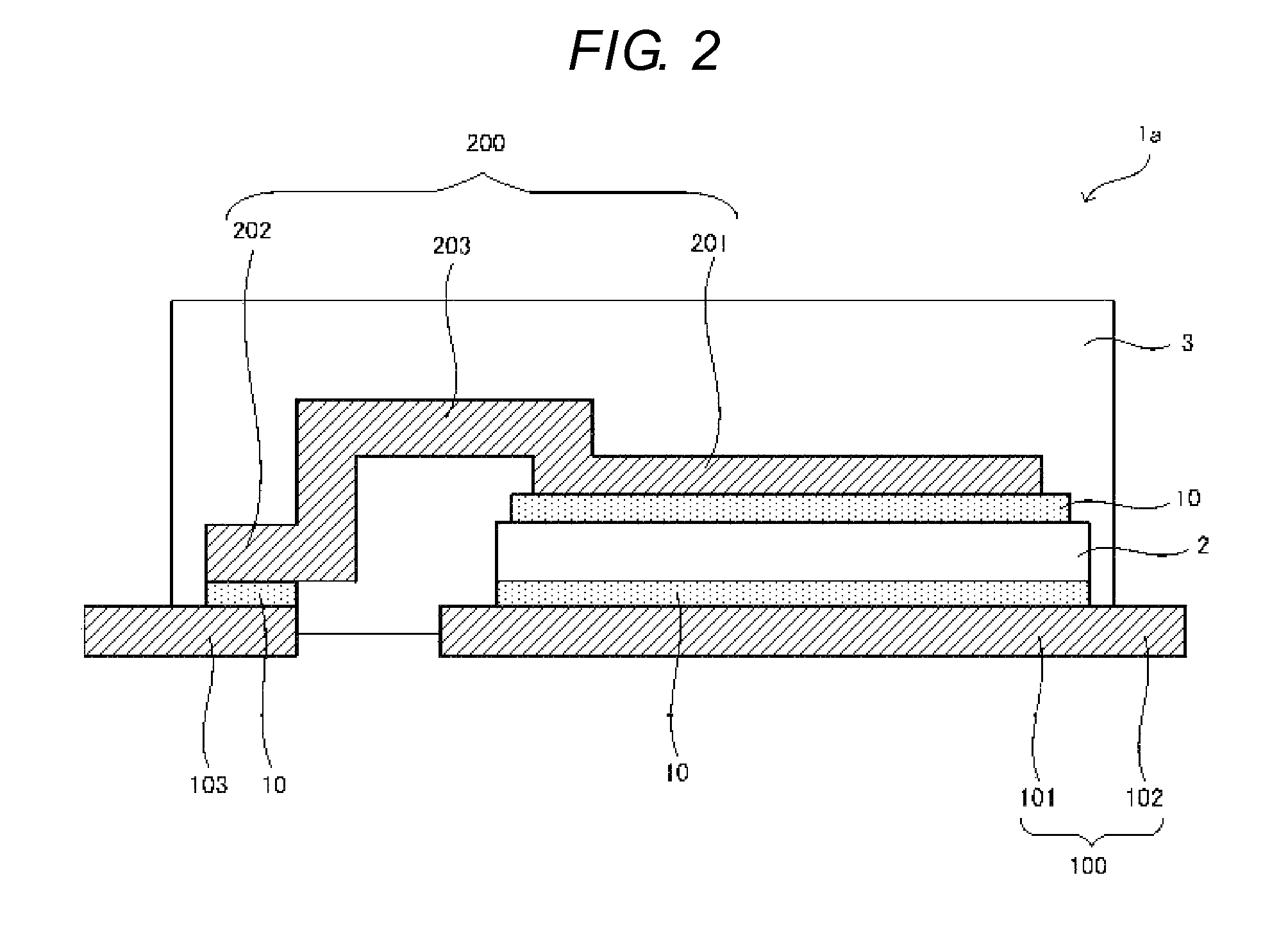
[0013]The structure of a semiconductor device 1a according to the present disclosure will be described with reference to FIGS. 1 and 2.

[0014]FIG. 1 shows a perspective view of the semiconductor device 1a according to the first embodiment of the present disclosure, and FIG. 2 shows a cross-sectional view illustrating a cross section along the line A-A′ of FIG. 1. Also, in the perspective view of FIG. 1, a resin 3 shown in FIG. 2 is omitted in FIG. 1 for clarity.

[0015]The semiconductor device 1a includes a semiconductor chip 2, the resin 3, a lead frame 100 (external electrode terminal), a source terminal 103, and a connector 200. The semiconductor chip 2 is, for example, a MOSFET having a vertically oriented electrode structure. In the present embodiment, the semiconductor chip 2 is described as the MOSFET; however, the semiconductor chip 2 may be an insulated gate bipolar transistor (IGBT). When the semiconductor chip 2 is a MOSFET, an upper electrode and a lower electrode constitut...

second embodiment

[0028]The structure of a semiconductor device 1b will be described with reference to FIGS. 3 and 4.

[0029]FIG. 3 shows a perspective view of the semiconductor device 1b according to the second embodiment, and FIG. 4 shows a cross-sectional view illustrating a cross section along the line B-B′ of FIG. 3.

[0030]As shown in FIGS. 3 and 4, the semiconductor device 1b according to the second embodiment is the same as the semiconductor device 1a according to the first embodiment with the following exception. A first metal plate 12 is provided between the semiconductor chip 2 and the chip contact surface 201. The other elements are the same as the semiconductor device 1a, and thus will not be described for brevity.

[0031]The first metal plate 12 is placed on the header 101 with a solder 10 (third connection material) interposed therebetween. A solder 10 (first connection material) is also interposed between the connector 200 and the first metal plate 12 such that the chip contact surface 201...

third embodiment

[0039]Also, in the third embodiment, an example in which the width of the lead frame contact plate 302 is greater than the widths of the chip contact surface 201 and the interconnecting portion 203 has been exemplified. However, the amount of the solder 10 applied to the source electrode 11 may be greater than the surface area of the lead frame contact plate 302 in contact with the source terminal 103. Alternatively, a second metal plate 400 may be provided between the lead frame contact plate 302 and the source electrode 11 as shown in FIG. 6. The second metal plate 400 may have a contact area between itself and the lead frame contact plate 302 and / or between itself and the source terminal 103 which is larger than the contact area of the lead frame contact plate 302 and the source electrode 11. The second metal plate 400 may be electrically connected to adjacent components via a solder (not shown).


PUM


Abstract

A semiconductor device includes a semiconductor chip having an electrode, a connector having a chip contact surface, an interconnecting portion, and an external electrode terminal contact surface, the chip contact surface being electrically connected to the electrode, and a first connection material disposed between the chip contact surface and the electrode, the first connecting material having a surface area that is greater than a surface area of the chip contact surface.

Description

CROSS-REFERENCE TO RELATED APPLICATION[0001]This application is based upon and claims the benefit of priority from Japanese Patent Application No. 2013-130030, filed Jun. 20, 2013, the entire contents of which are incorporated herein by reference.FIELD[0002]Embodiments described herein relate generally to a semiconductor device.BACKGROUND[0003]Conventionally, semiconductor devices include semiconductor chips including metal oxide semiconductor field effect transistors (MOSFETs) having vertically oriented electrode structures with copper connectors, or the like, that are connected to lead frames or external electrode terminals. In these devices, copper connectors having the same size and shape (i.e. standard connectors) are used in order to improve the efficiencies of managing the inventory to manufacture different products. However, the sizes of semiconductor chips may be different and thus the contact area of the standard connector may not be suitable for connection with differentl...

Claims


Application Information

Patent Timeline
IPC IPC(8): H01L23/495H01L23/00
CPCH01L24/29H01L23/49524H01L23/49562H01L24/40H01L23/49513H01L24/32H01L24/33H01L24/37H01L24/73H01L2224/04026H01L2224/04034H01L2224/06181H01L2224/29007H01L2224/29083H01L2224/29111H01L2224/29116H01L2224/29139H01L2224/29144H01L2224/29147H01L2224/32245H01L2224/3303H01L2224/33181H01L2224/37144H01L2224/37147H01L2224/40247H01L2224/40491H01L2224/73263H01L2924/1305H01L2924/13055H01L2924/13091H01L2924/00H01L2224/40095H01L2924/181H01L2224/84801H01L2224/83801H01L24/41H01L2224/0603H01L2924/00012H01L23/49517H01L23/49527H01L24/34H01L24/39
Inventor MIYAKAWA, TAKESHI
Owner KK TOSHIBA
Why Eureka
Try Eureka