
Electromagnetic shielding structures for selectively shielding components on a substrate

a technology of electromagnetic shielding and components, applied in the field of electromagnetic shielding structures, can solve problems such as the potential to generate electromagnetic interference for other components, and achieve the effect of reducing device dimensions and preventing electrical shorting

Active Publication Date: 2015-11-03
APPLE INC
View PDF92 Cites 18 Cited by
  • Summary
  • Abstract
  • Description
  • Claims
  • Application Information

AI Technical Summary

Benefits of technology

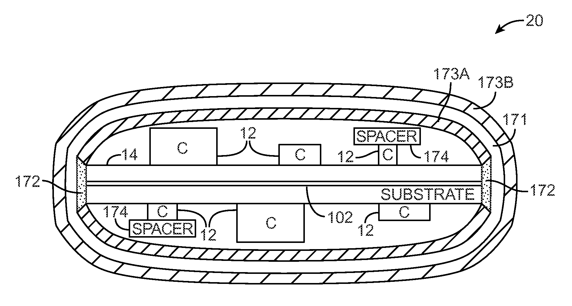
This patent describes a way to protect sensitive electrical components from electromagnetic interference. This is done by using insulating materials and conductive materials to create shielding structures around the components. The shielding structures can be formed using manufacturing tools like molding and cutting tools, as well as solder walls and metal fences. The substrate can also have sacrificial regions to allow for manufacturing tolerances and to grip the substrate. The insulating materials provide structural support to the conductive layer and help prevent shorts between components. This technique helps to create an efficient and effective electromagnetic shield for components.

Problems solved by technology

The electrical components may be sensitive to electromagnetic interference and may have the potential to generate electromagnetic interference for other components.

Method used


Image

  • Electromagnetic shielding structures for selectively shielding components on a substrate
  • Electromagnetic shielding structures for selectively shielding components on a substrate
  • Electromagnetic shielding structures for selectively shielding components on a substrate

Examples


Embodiment Construction

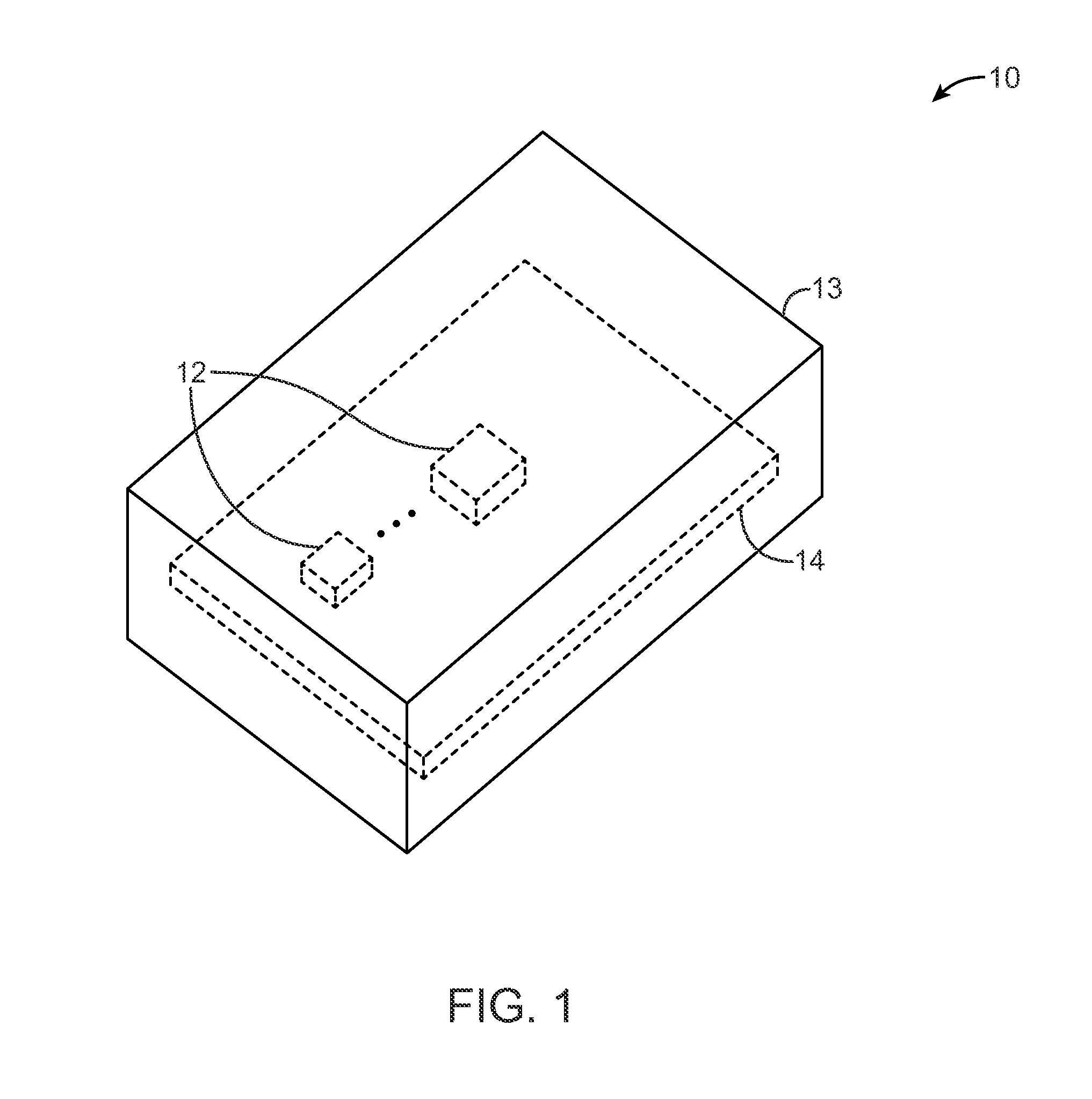
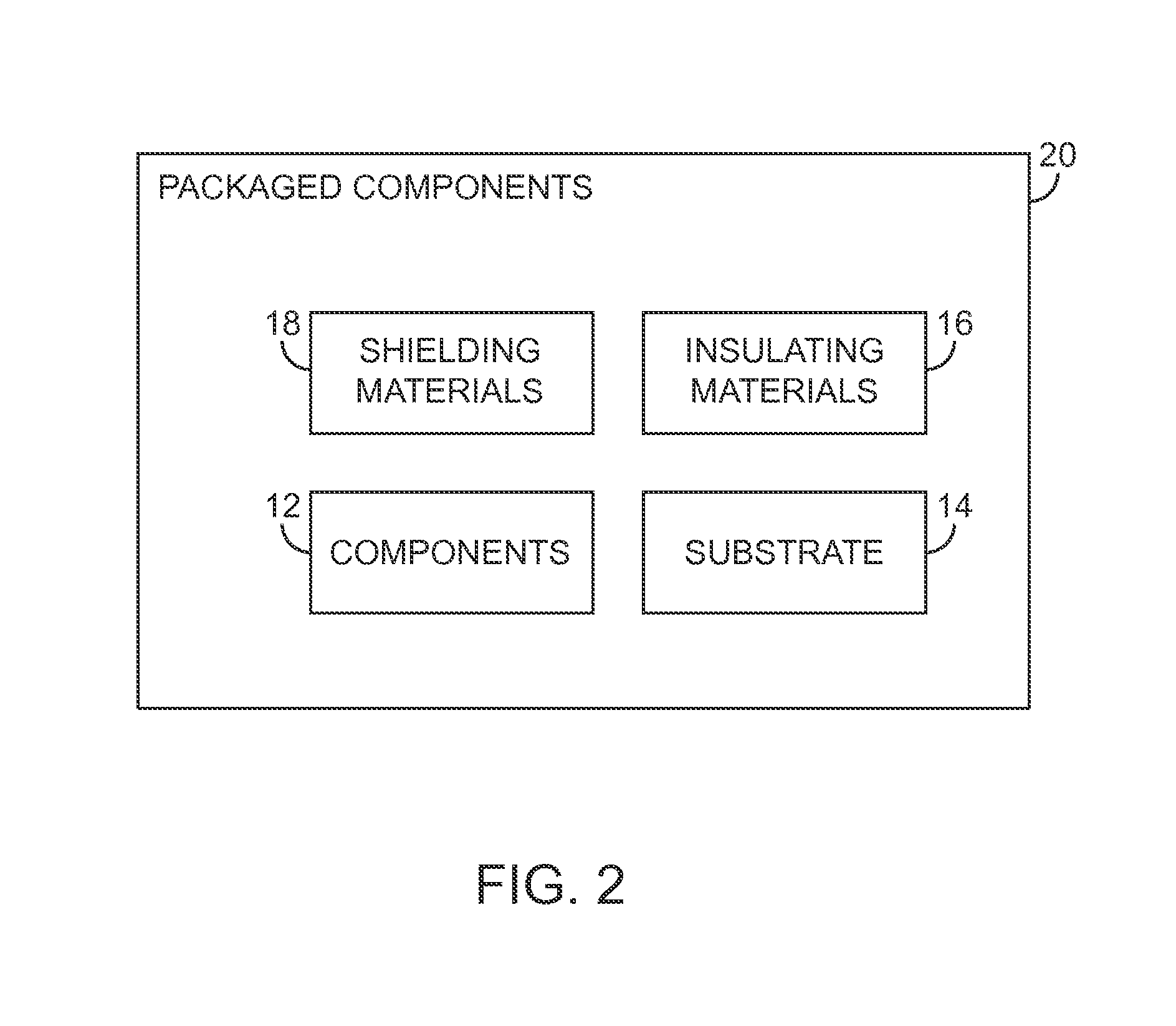
[0040]This relates to shielding structures for electrical components. The shielding structures may include radio-frequency shielding structures and / or magnetic shielding structures. The electrical components that are shielded by the shielding structures may be components such as integrated circuits that operate in radio-frequency bands (e.g., transceiver integrated circuits, memory circuits and other circuits with clocks that produce signals with fundamentals or harmonics in radio-frequency bands, etc.). Shielded components may also include circuitry formed from one or more discrete components such as inductors, capacitors, and resistors, switches, etc. The electrical components that are shielded may be aggressors (components that produce radio-frequency or magnetic signal interference) and / or victims (components that are sensitive to interference that is received from external sources).

[0041]The shielding structures may help to reduce interference from electromagnetic signals and m...


PUM

PropertyMeasurementUnit
Electrical conductoraaaaaaaaaa
Electromagnetismaaaaaaaaaa
aaaaaaaaaa

Abstract

Electronic components on a substrate may be shielded using electromagnetic shielding structures. Insulating materials may be used to provide structural support and to help prevent electrical shorting between conductive materials and the components. The shielding structures may include compartments formed using metal fences that surround selected components or by injection molding plastic. The shielding structures may be formed using metal foil wrapped over the components and the substrate. Electronic components may be tested using test posts or traces to identify components that are faulty. The test posts or traces may be deposited on the substrate and may be used to convey test signals between test equipment and the components. After successful testing, the test posts may be permanently shielded. Alternatively, temporary shielding structures may be used to allow testing of individual components before an electronic device is fully assembled.

Description

[0001]This application claims the benefit of provisional patent application No. 61 / 495,348, filed Jun. 9, 2011, which is hereby incorporated by reference herein in its entirety.BACKGROUND[0002]This relates generally to mitigating radio-frequency interference and, more particularly, to electromagnetic shielding structures that help isolate radio-frequency circuitry from radio-frequency interference.[0003]Electronic devices such as computers, cellular telephones, and other devices often contain circuitry that requires electromagnetic shielding. For example, some electronic devices include radio-frequency transceiver circuits that are susceptible to radio-frequency interference. Electronic devices may also include memory and other components that use clock signals during normal operation. If care is not taken, signals from one circuit may interfere with the proper operation of another circuit. For example, a clock signal or a clock signal harmonic that falls within the operating band o...

Claims


Application Information

Patent Timeline
IPC IPC(8): H05K9/00H05K1/02H01L23/552H01L25/065
CPCH05K1/0218H01L23/552H05K9/003H05K9/0026H05K9/0043H01L25/0655H01L2924/0002H01L2924/14H01L2924/15192H01L2924/1815H01L2924/19041H01L2924/19043H01L2924/19105H05K9/0033H05K9/0037Y10T29/49004Y10T29/4913Y10T29/49146H01L2924/00H01L2924/3025H05K9/0031H05K9/0024H05K1/02H05K9/00
Inventor FOSTER, JAMES H.BILANSKI, JAMES W.SALEHI, AMIRCHANDHRASEKHAR, RAMAMURTHYWEBB, NICHOLAS UNGER
Owner APPLE INC
Learn More