Method and apparatus for delay compensation in data transmission

a delay compensation and data technology, applied in the field of integrated circuits (ics), can solve problems such as data strobe signals being subject to delay, data mismatches at the receiver, and insertion delay at the memory

Active Publication Date: 2015-12-08
APPLE INC
View PDF18 Cites 5 Cited by
  • Summary
  • Abstract
  • Description
  • Claims
  • Application Information

AI Technical Summary

Benefits of technology

[0006]A method and apparatus for delay compensation in data transmission is disclosed. In one embodiment, an IC is configured to transmit data along with a clock signal to which the data is synchronized at the receiver. The IC includes a delay circuit configured to receive the data, which is transmitted in beats. The delay circuit includes a number of pipelines corresponding to the number of beats. Beats of data input into the delay circuit are routed to particular ones of the pipelines in accordance with a desired amount of delay. The delay applied to the data may be set to a desired alignment between the data and the clock signal at the receiver and to compensate for inherent delays that affect the clock signal.
[0008]The memory controller may also include clock generation circuitry that includes one or more delay locked loops (DLLs). One of the DLLs may be used to generate the data strobe signal based on another clock signal received thereby. The alignment at the memory between the data and the data strobe signal may be adjusted in part by adjusting a delay applied by the DLL that generates the data strobe signal. The adjustment of the delay applied by the DLL may be limited in order to prevent setup and / or hold time violations in the clocked storage circuits of the memory. Thus, the delay circuit may be used to apply delay to the data to provide additional compensation for the insertion delay.

Problems solved by technology

During such data transfers, inherent delays in the signal paths for both the data and clock signals can cause timing mismatches at the receiver.
The data strobe signal may be subject to a delay (known as an insertion delay) at the memory due to various factors, such as its fan out to the various clocked storage circuits.

Method used


Image

  • Method and apparatus for delay compensation in data transmission
  • Method and apparatus for delay compensation in data transmission
  • Method and apparatus for delay compensation in data transmission

Examples


Embodiment Construction

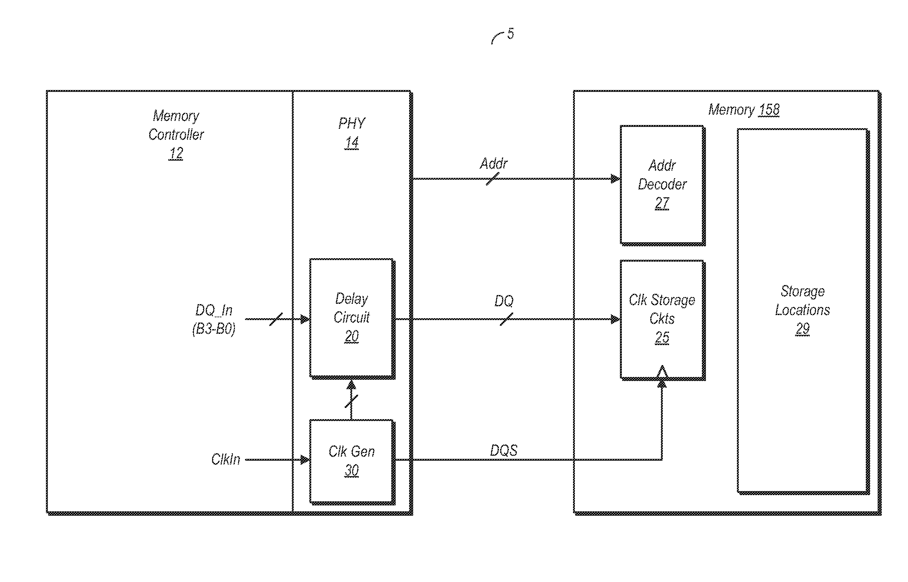
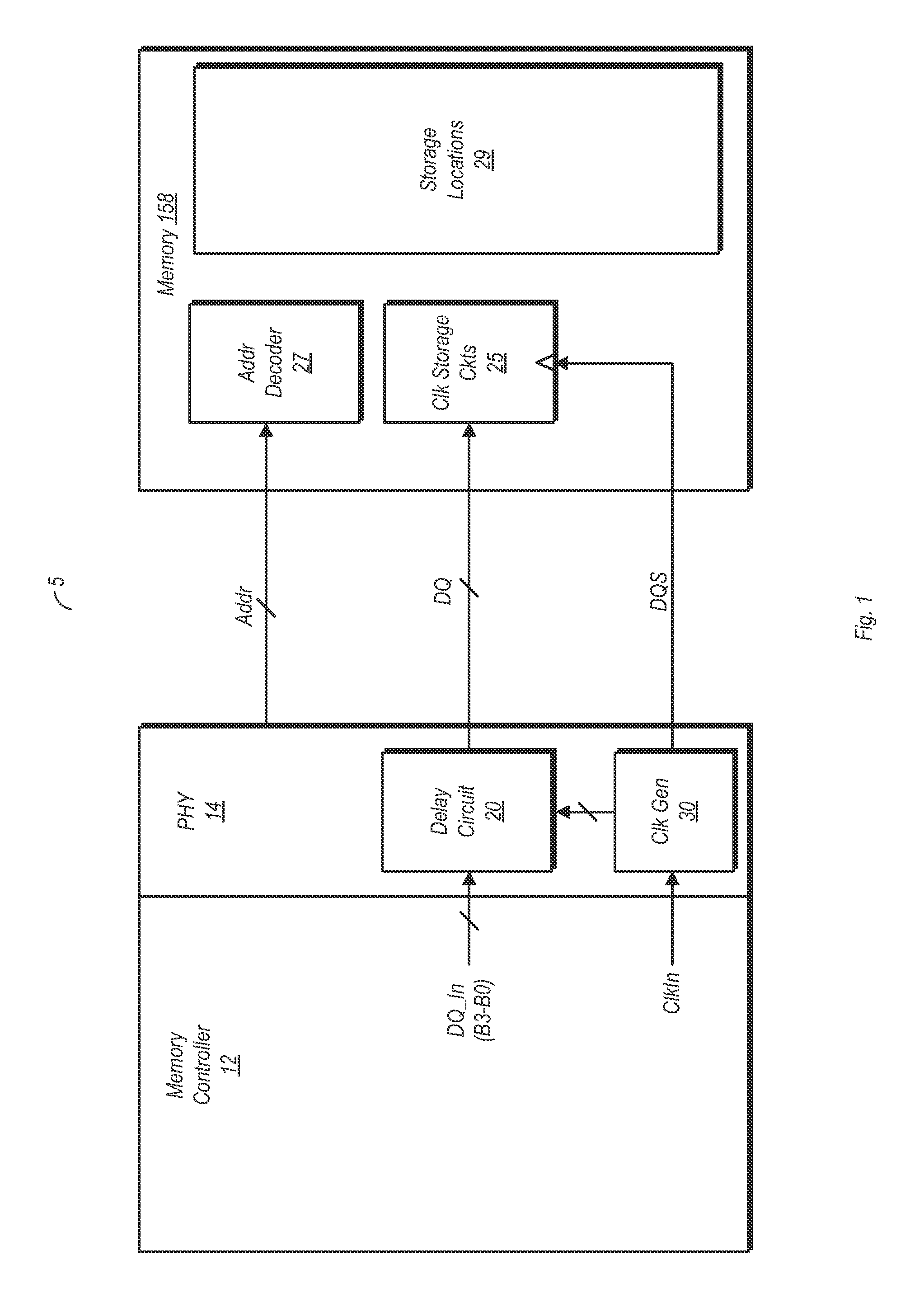
[0018]Turning now to FIG. 1, a block diagram of a system having a memory controller and a memory is shown. In the embodiment shown, system 5 includes a memory controller 12 and a memory 158. The memory controller 12 includes a physical layer 14 which is used for interfacing with memory 158. Memory 158 includes an address decoder 27, a number of clocked storage circuits 25, and a number of storage locations 29.

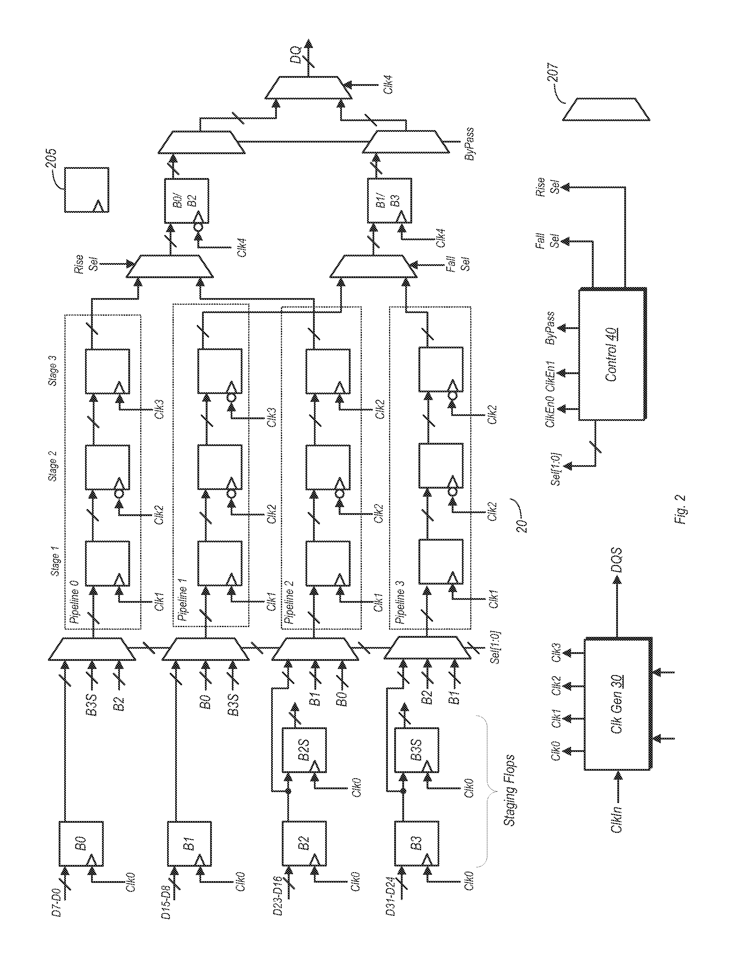
[0019]Physical layer 14 includes a delay circuit 20 and a clock generation circuit 30. Delay circuit 20 in the embodiment shown is coupled to receive data from other circuitry in the memory controller and provide a delay thereto before its transmission to memory 158. In this particular embodiment, the data may be transferred in beats. For example, a 32-bit data word may be transmitted in four beats of eight bits each. Accordingly, the data input (DQ_In) of delay circuit 20 is configured to receive four beats of data, B3-B0, in this particular embodiments. It is noted that trans...


PUM


Abstract

A method and apparatus for delay compensation in data transmission is disclosed. In one embodiment, an IC is configured to transmit data along with a clock signal to which the data is synchronized at the receiver. The IC includes a delay circuit configured to receive the data, which is transmitted in beats. The delay circuit includes a number of pipelines corresponding to the number of beats. Beats of data input into the delay circuit are routed to particular ones of the pipelines in accordance with a desired amount of delay. The delay applied to the data may be set to align the data with the clock signal at the receiver and to compensate for inherent delays that affect the clock signal.

Description

BACKGROUND[0001]1. Technical Field[0002]This disclosure is directed to integrated circuits (ICs), and more particularly, to delay compensation in data transmissions that occur in ICs.[0003]2. Description of the Related Art[0004]In computers and other electronic systems, data is often transmitted synchronous with a clock signal. For example, data to be written to a memory may be sent from an IC to a memory on another chip along with a clock signal. In another example, data may be transferred within an IC, from a processor core to an on-chip memory, along with a clock signal. During such data transfers, inherent delays in the signal paths for both the data and clock signals can cause timing mismatches at the receiver. Accordingly, compensation circuitry is often provided at the receiver in order to apply delays to ensure data is properly captured.[0005]One common type of circuit used for implementing delays to compensate for timing mismatches is the delay locked loop (DLL). For exampl...

Claims


Application Information

Patent Timeline
Patent Type & Authority Patents(United States)
IPC IPC(8): H04L7/00H03K5/14H03L7/08
CPCH04L7/0041H03L7/08H03K5/14H03K5/133H03K2005/00234
Inventor NOTANI, RAKESH L.
Owner APPLE INC
Why Eureka
Try Eureka